28
Plasma TV Service Manual
05/01/2006
V
SSD7
G11
P
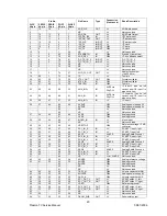
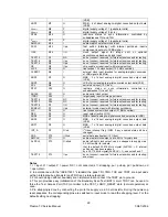
digital ground 7 (peripheral cells)
IPD1
G12
O
MSB - 6 of image port data output
HPD7
G13
I/O
MSB of host port data I/O, extended C
B
-C
R
R input for
expansion port, extended C
B
-C
R
output for image port
IPD0
G14
O
LSB of image port data output
AI2D
H1
I
differential input for ADC channel 2 (pins AI24 to AI21)
AI23
H2
I
analog input 23
V
SSA2
H3
P
ground for analog inputs AI2x
V
DDA2
H4
P
analog supply voltage for analog inputs AI2x
IPD2
H11
O
MSB - 5 of image port data output
V
DDD7
H12
P
digital supply voltage 7 (peripheral cells)
IPD4
H13
O
MSB - 3 of image port data output
IPD3
H14
O
MSB - 4 of image port data output
V
DDA2A
J1
P
analog supply voltage for analog inputs AI2x
AI11
J2
I
analog input 11
AI24
J3
I
analog input 24
V
SSA1
J4
P
ground for analog inputs AI1x
V
SSD8
J11
P
digital ground 8 (core)
V
DDD8
J12
P
digital supply voltage 8 (core)
IPD6
J13
O
MSB
−
1 of image port data output
IPD5
J14
O
MSB
−
2 of image port data output
AI12
K1
I
analog input 12
AI13
K2
I
analog input 13
AI1D
K3
I
differential input for ADC channel 1 (pins AI14 to AI11)
V
DDA1
K4
P
analog supply voltage for analog inputs AI1x (3.3 V)
IPD7
K11
O
MSB of image port data output
IGPH
K12
O
multi purpose horizontal reference output signal; image port
(controlled by subaddresses 84H and 85H)
IGP1
K13
O
general purpose output signal 1; image port (controlled by
subaddresses 84H and 85H)
IGPV
K14
O
multi purpose vertical reference output signal; image port
(controlled by subaddresses 84H and 85H)
V
DDA1A
L1
P
analog supply voltage for analog inputs AI1x (3.3 V)
AGNDA
L2
P
analog signal ground
AI14
L3
I
analog input 14
V
SSD9
L4
P
digital ground 9 (peripheral cells)
V
SSD10
L5
P
digital ground 10 (core)
ADP6
L6
O
MSB - 2 of direct analog-to-digital converted output data
(VSB)
ADP3
L7
O
MSB - 5 of direct analog-to-digital converted output data
(VSB)
V
SSD11
L8
P
digital ground 11 (peripheral cells)
V
SSD12
L9
P
digital ground 12 (core)
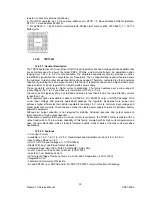
RTCO
L10
O/st/pd
real-time control output; contains information about actual
system clock frequency, field rate, odd/even sequence,
decoder status, subcarrier frequency and phase and PAL
sequence; the RTCO pin is enabled via I
2
C-bus bit RTCE;
see notes 5, 6
V
SSD13
L11
P
digital ground 13 (peripheral cells)
ITRI
L12
I/(O)
image port output control signal, affects all input port pins
inclusive ICLK, enable and active polarity is under software
control (bits IPE in subaddress 87H); output path used for
testing: scan output
IDQ
L13
O
output data qualifier for image port (optional: gated clock
output)
IGP0
L14
O
general purpose output signal 0; image port (controlled by
subaddresses 84H and 85H)
AOUT
M1
O
analog test output (do not connect)
V
SSA0
M2
P
ground for internal Clock Generation Circuit (CGC)
V
DDA0
M3
P
analog supply voltage (3.3 V) for internal clock generation
circuit
V
DDD9
M4 P
digital supply voltage 9 (peripheral cells)
V
DDD10
M5 P
digital supply voltage 10 (core)
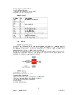
ADP7
M6
O
MSB
−
1 of direct analog-to-digital converted output data
Summary of Contents for 17MB11
Page 1: ...50 PLASMA TV 17MB11 SERVICE MANUAL...
Page 50: ...47 Plasma TV Service Manual 25 08 2005 15 CIRCUIT DIAGRAMS...
Page 51: ...48 Plasma TV Service Manual 25 08 2005...
Page 52: ...49 Plasma TV Service Manual 25 08 2005...
Page 53: ...50 Plasma TV Service Manual 25 08 2005...
Page 54: ...51 Plasma TV Service Manual 25 08 2005...
Page 55: ...52 Plasma TV Service Manual 25 08 2005...
Page 56: ...53 Plasma TV Service Manual 25 08 2005...
Page 57: ...54 Plasma TV Service Manual 25 08 2005...


