background image

32” TFT TV Service Manual 

06/03/2006


12.4. ST24LC21 

12.4.1. Description 

The ST24LC21 is a 1K bit electrically erasable programmable memory (EEPROM), organized by 8 bits. 
This device can operate in two modes: Transmit Only mode and I

2

C bidirectional mode. When powered, 

the device is in Transmit Only mode with EEPROM data clocked out from the rising edge of the signal 
applied on VCLK. The device will switch to the I

2

C bidirectional mode upon the falling edge of the signal 

applied on SCL pin. The ST24LC21 can not switch from the I

2

C bidirectional mode to the Transmit Only 

mode (except when the power supply is removed). The device operates with a power supply value as low 
as 2.5V. Both Plastic Dual-in-Line and Plastic Small Outline packages are available. 

12.4.2. Features 

• 1 million Erase/Write cycles 
• 40 years data retention 
• 2.5V to 5.5V single supply voltage 
• 400k Hz compatibility over the full range of supply voltage 
• Two wire serial interface I

2

C bus compatible 

• Page Write (Up To 8 Bytes) 
• Byte, random and sequential read modes 
• Self timed programming cycle 
• Automatic address incrementing 
• Enhanced ESD/Latch up 
• Performances 

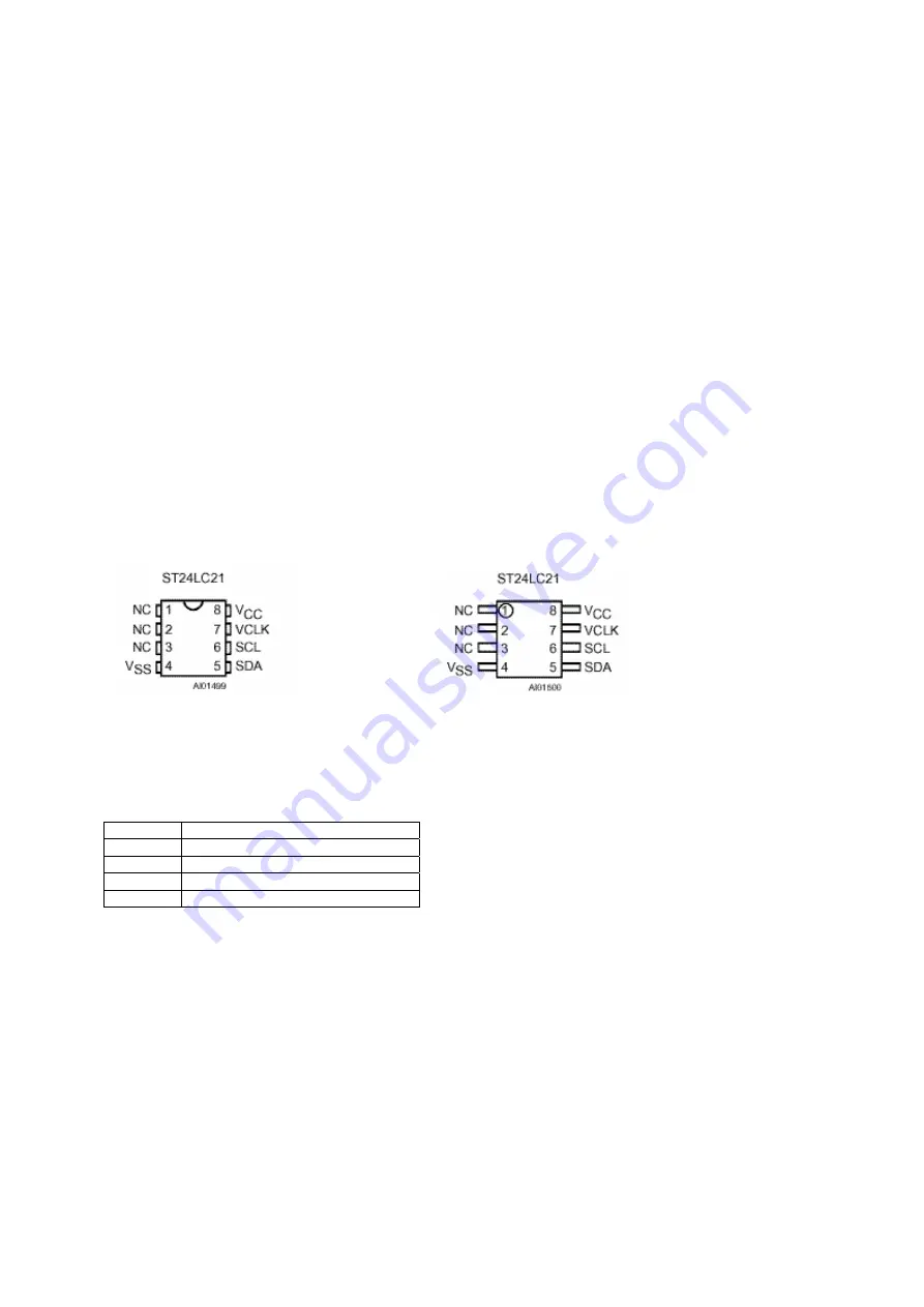
12.4.3. Pin 

connections 


DIP Pin connections 

CO Pin connections 

 
NC: Not connected 
 

Signal names 


SDA Serial 

data 

Address Input/Output 

SCL 

Serial Clock (I

2

C mode) 

V

cc

 Supply 

voltage 

V

ss

 Ground 

VCLK 

Clock transmit only mode 


Summary of Contents for 17MB18P-3

Page 1: ......

Page 2: ...12 1 1 General Description 5 12 1 2 Features 5 12 1 3 Applications 5 12 1 4 Connection Diagrams 5 12 2 LM2576 6 12 2 1 General Description 6 12 2 2 Features 6 12 2 3 Pin description 6 12 3 LM317T 7 12 3 1 Description 7 12 3 2 Features 7 12 4 ST24LC21 8 12 4 1 Description 8 12 4 2 Features 8 12 4 3 Pin connections 8 12 5 TEA5114A 9 12 5 1 General description 9 12 5 2 Features 9 12 5 3 Pin Connectio...

Page 3: ...15 MC141585 22 12 15 1 General description 22 12 15 2 Features 22 12 15 3 Pin Description 22 12 16 MC34063 24 12 16 1 Description 24 12 16 2 Features 24 12 16 3 Pin connections 24 12 17 MSP34X0G MSP3410G 25 12 17 1 Introduction 25 12 17 2 Features 25 12 17 3 Pin connections 26 12 18 DS90C385 28 12 18 1 General Description 28 12 18 2 Features 28 12 18 3 Pinning 28 12 19 NDS8947 29 12 19 1 General D...

Page 4: ...mpedance has been designed for direct drive of a wide variety of SAW filters with sufficient suppression of triple transient Features of UV1316 1 Member of the UV1300 family small sized UHF VHF tuners 2 Systems CCIR B G H L L I and I OIRT D K 3 Digitally controlled PLL tuning via I2 C bus 4 Off air channels S cable channels and Hyper band 5 Compact size 6 Complies to CENELEC EN55020 and EN55013 Pi...

Page 5: ...he 6 outputs Each output can be switched on only one of each input On each input an alignment of the lowest level of the signal is made bottom of sync top for CVBS or black level for RGB signals Each nominal gain between any input and output is 6 5dB For D2MAC or Chroma signal the alignment is switched off by forcing with an external resistor bridge 5VDC on the input Each input can be used as a no...

Page 6: ...VPS PDC WSS Acquisition Buffer directly accessible via MOVX UP to 16KByte on Chip Extended RAM XRAM consisting of 1 Kilobyte on chip ACQ buffer RAM access via MOVX 1 Kilobyte on chip extended RAM XRAM access via MOVX for user software 3 Kilobyte Display Memory 8 5 Display Features ROM Character set supports all East and West European Languages in single device Mosaic Graphic Character Set Parallel...

Page 7: ...le in P SDIP 52 9 SERIAL ACCESS CMOS 16K 2048 8 EEPROM ST24C16 The ST24C16 is a 16Kbit electrically erasable programmable memory EEPROM organised as 8 blocks of 256 8 bits The memory is compatible with the I C standard two wire serial interface which uses a bi directional data bus and serial clock The memory carries a built in 4 bit unique device identification code 1010 corresponding to the I C b...

Page 8: ... 2 5V 2 85V 3 3V and 5V The LM1117 offers current limiting and thermal shutdown Its circuit includes a zener trimmed bandgap reference to as sure output voltage accuracy to within 1 The LM1117 series is available in SOT 223 TO 220 and TO 252 D PAK packages A minimum of 10µF tantalum capacitor is required at the output to improve the transient response and stability 12 1 2 Features Available in 1 8...

Page 9: ...nk is required or its size could be reduced dramatically A standard series of inductors optimized for use with the LM2576 are available from several different manufacturers This feature greatly simplifies the design of switch mode power supplies The LM2576 features include a guaranteed 4 tolerance on output voltage within specified input voltages and output load conditions and 10 on the oscillator...

Page 10: ... LM317 serves a wide variety of applications including local on card regulation This device can also be used to make a programmable output regulator or by connecting a fixed resistor between the adjustment and output the LM317 can be used as a precision current regulator 12 3 2 Features Output Current in Excess of 1 5 A Output Adjustable between 1 2 V and 37 V Internal Thermal Overload Protection ...

Page 11: ...ly mode except when the power supply is removed The device operates with a power supply value as low as 2 5V Both Plastic Dual in Line and Plastic Small Outline packages are available 12 4 2 Features 1 million Erase Write cycles 40 years data retention 2 5V to 5 5V single supply voltage 400k Hz compatibility over the full range of supply voltage Two wire serial interface I2 C bus compatible Page W...

Page 12: ...e same reference voltage on each input in order to have no differential voltage when switching two RGB generators An AC output signal higher than 2 Vpp makes gain going slowly down to 0dBto protect the TV set video amplifier from saturation Fast blanking output is a logical OR between FB1 Pin 8 and FB2 Pin 10 12 5 2 Features 25MHz Bandwidth Crosstalk 55dB Short circuit to ground or VCC protected A...

Page 13: ...guration In other case 1 word of 16 bits is necessary to determine one configuration 12 6 2 Features 20MHz Bandwidth Cascadable with another TEA6415C Internal address can be changed by pin 7 voltage 8 Inputs CVBS RGB MAC CHROMA 6 Outputs Possibility of MAC or chroma signal for each input by switching off the clamp with an external resistor bridge Bus controlled 6 5dB gain between any input and out...

Page 14: ... 80 pin PQFP package 12 7 2 Pin Connections and Short Descriptions NC not connected LV if not used leave vacant X obligatory connect as described in circuit diagram SUPPLYA 4 75 5 25 V SUPPLYD 3 15 3 45 V Pin No PQFP 80 pin Pin Name Type Connection if not used Short Description 1 B1 CB1IN IN VREF Blue1 Cb1 Analog Component Input 2 G1 Y1IN IN VREF Green1 Y1 Analog Component Input 3 R1 CR1IN IN VREF...

Page 15: ... Front Sync Horizontal Clamp Pulse Front End Horizontal Sync Output 56 MSY HS IN OUT LV Main Sync Horizontal Sync Pulse 57 VS OUT LV Vertical Sync Pulse 58 FPDAT VSYA IN OUT LV Front End Back End Data Front End Vertical Sync Output 59 VSTBYY SUPPLYA X Standby Supply Voltage 60 CLK5 OUT LV CCU 5 MHz Clock Output 61 NC LV or GNDD Not Connected 62 XTAL1 IN X Analog Crystal Input 63 XTAL2 OUT X Analog...

Page 16: ...bilities based on parallel attributes and Pixel oriented characters DRCS The 8 bit Microcontroller runs at 360 ns cycle time min Controller with dedicated hardware does most of the internal TTX acquisition processing transfers data to from external memory interface and receives transmits data via I2 C firmware user interface The slicer combined with dedicated hardware stores TTX data in a VBI buff...

Page 17: ...2 eliminates the need for external heatsinks when playing music 12 9 2 Features 9 W Ch Into an 8 Ω Load From 12 V Supply Efficient Class D Operation Eliminates Heatsinks and Reduces Power Supply Requirements 32 Step DC Volume Control From 40 dB to 36 dB Line Outputs For External Headphone Amplifier With Volume Control Regulated 5 V Supply Output for Powering TPA6110A2 Space Saving Thermally Enhanc...

Page 18: ...Frequency Control AFC detector with 4 bit digital to analog converter AFC bits via I2 C bus readable TakeOver Point TOP adjustable via I2 C bus or alternatively with potentiometer Fully integrated sound carrier trap for 4 5 5 5 6 0 and 6 5 MHz controlled by FM PLL oscillator Sound IF SIF input for single reference Quasi Split Sound QSS mode PLL controlled SIF AGC for gain controlled SIF amplifier ...

Page 19: ...xcellent power supply ripple rejection Low power consumption Short circuit resistant High performance high signal to noise ratio High slew rate Low distortion Large output voltage swing 12 11 3 Pinning SYMBOL PIN DESCRIPTION PIN VALUE OUTA 1 Output A Voltage swing Min 0 75V Max 4 25V INA neg 2 Inverting input A Vo clip Min 1400mVrms INA pos 3 Non inverting input A 2 5V VSS 4 Negative supply 0V INB...

Page 20: ...greater than most analog switches offered today A single 5V supply is all that is required for operation The PI5V330 offers a high performance low cost solution to switch between video sources The application section describes the PI5V330 replacing the HC4053 multiplier and buffer amplifier 12 12 2 Features High performance low cost solution to switch between video sources Wide bandwidth 200 MHz L...

Page 21: ...The design kit is complete with hardware and software Software includes G Probe debug software G Wizard register calculator and G TV application source code The 6015RD1 is a related reference board that outputs analog YpbPr RGB 12 13 2 Features Dual channel gm6015 based LCD TV system Industry leading Crystal Cinema Plus video scan conversion Inputs i Component analog YPbPr RGB ii 480 576I 480 576P...

Page 22: ...vided in a space saving 80 lead LQFP surface mount plastic package and is specified over the 0C to 70C temperature range 12 14 2 Features 140 MSPS Maximum Conversion Rate 300 MHz Analog Bandwidth 0 5 V to 1 0 V Analog Input Range 500 ps p p PLL Clock Jitter at 110 MSPS 3 3 V Power Supply Full Sync Processing Sync Detect for Plugging Midscale Clamping Power Down Mode Low Power 500 mW Typical 4 2 2 ...

Page 23: ...ctive The input includes a Schmitt trigger for noise immunity with a nominal input threshold of 1 5 V VSYNC Vertical Sync Input This is the input for vertical sync SOGIN Sync on Green Input This input is provided to assist with processing signals with embedded sync typically on the GREEN channel The pin is connected to a high speed comparator with an internally generated threshold The threshold le...

Page 24: ...oper operation the pixel clock generator PLL requires an external filter Connect the filter shown in Figure 6 to this pin For optimal performance minimize noise and parasitics on this node POWER SUPPLY VD Main Power Supply These pins supply power to the main elements of the circuit They should be as quiet and filtered as possible VDD Digital Output Power Supply A large number of output pins up to ...

Page 25: ...ght of character and row to row spacing and full screen erasing and Fade In Fade Out are also incorporated There are 8 color selections for any individual character display with row intensity attribute and window intensity attribute to expand the color mixture on OSD menu 12 15 2 Features Totally 512 Fonts Including 496 Standard Fonts and 16 Multi Color Fonts 10x18 or 12x18 Font Matrix Selection M...

Page 26: ...Data is read at the rising edge of each clock signal VDD Pin 9 This is the power pin for the digital logic of the chip VSYNC Pin 10 Similar to Pin 5 this pin inputs a vertical synchronize signal to synchronize the vertical control circuit It is negative polarity by default VDD I Pin 11 This is the voltage supply of RGB outputs when low intensity of Windows ROW is selected The RBG output level woul...

Page 27: ...d duty cycle oscillator with an active current limit circuit driver and high current output switch This series was specifically designed to be incorporated in Step Down and Step Up and Voltage Inverting applications with a minimum number of external components 12 16 2 Features Operation from 3 0 V to 40 V Input Low Standby Current Current Limiting Output Switch Current to 1 5 A Output Voltage Adju...

Page 28: ...further simplifies controlling software Standard selection requires a single I C transmission only The MSP 34x0G has built in automatic functions The IC is able to detect the actual sound standard automatically Automatic Standard Detection Furthermore pilot levels and identification signals can be evaluated internally with subsequent switching between mono stereo bilingual no I C interaction is ne...

Page 29: ...0 8 1 64 NC LV Not connected 11 7 6 80 63 STANDBYQ IN OBL Stand by low active 12 6 5 79 62 ADR_SEL IN OBL I 2 C bus address select 13 5 4 78 61 D_CTR_I O_0 IN OUT LV D_CTR_I O_0 14 4 3 77 60 D_CTR_I O_1 IN OUT LV D_CTR_I O_1 15 3 76 59 NC LV Not connected 16 2 75 58 NC LV Not connected 17 NC LV Not connected 18 1 2 74 57 AUD_CL_OUT OUT LV Audio clock output 18 432 MHz 19 64 1 73 56 TP LV Test pin ...

Page 30: ...LV SCART output 2 left 51 33 27 33 25 SC2_OUT_R OUT LV SCART output 2 right 52 32 NC LV Not connected 53 32 31 24 NC LV Not connected 54 31 26 30 23 DACM_SUB OUT LV Subwoofer output 55 30 29 22 NC LV Not connected 56 29 25 28 21 DACM_L OUT LV Loudspeaker out left 57 28 24 27 20 DACM_R OUT LV Loudspeaker out right 58 27 23 26 19 VREF2 OBL Reference ground 2 59 26 22 25 18 DACA_L OUT LV Headphone ou...

Page 31: ...ge strobe through a dedicated pin A Rising edge or Falling edge strobe transmitter will interoperate with a Falling edge strobe Receiver DS90CF386 DS90CF366 without any translation logic The DS90C385 is also offered in a 64 ball 0 8mm fine pitch ball grid array FBGA package which provides a 44 reduction in PCB footprint compared to the TSSOP package This chipset is an ideal means to solve EMI and ...

Page 32: ... and provide superior switching performance These devices are particularly suited for low voltage applications such as notebook computer power management and other battery powered circuits where fast switching low in line power loss and resistance to transients are needed 12 19 2 Features 4A 30V RDS ON 0 065W VGS 10V RDS ON 0 1W VGS 4 5V High density cell design for extremely low RDS ON High power...

Page 33: ...he following menu appears on the screen After entering the Service menu you can access its items by pressing buttons In order to enter selected menu use buttons To exit the service menu press M button Entire service menu parameters of TFT TV are listed below 13 1 ADJUST MENU SETTINGS In order to enter Adjust menu move the cursor to Adjust parameter by pressing buttons in Service Menu and press but...

Page 34: ...On Off If ON TV starts with APS menu at Start up A P S On Off Enables disables Automatic Programming System Headphone On Off Enables disables the usage of the HP and HP related items in Sound menu Vsr On Off Enables disables Vsr DBE On Off Enables disables DBE Subwoofer On Off Enables disables Subwoofer Lineout On Off Enables disables Lineout Dolby prologic On Off Enables disables dolby prologic s...

Page 35: ...les NZ Standard NM On Off Enables disables NM Standard FM Prs Avl On Adjusts the FM Prescaler value when Automatic Volume Levelling is On Min Value 0000 00000 Max Value 00FF 00255 Options Equalizer BG DK I L L AUS NZ NM FM Prs Avl On 017 Off Options FM Prs Avl On Nicam Prs Avl On Scart Prs Avl On Scart Volume Avl On FM Prs Avl Off Nicam Prs Avl Off Scart Prs Avl Off Scart Volume Avl Off HOTEL VoD ...

Page 36: ...ts the FM Prescaler value when Automatic Volume Levelling is Off Min Value 0000 00000 Max Value 00FF 00255 Nicam Prs Avl Off Adjusts the Nicam Prescaler value when Automatic Volume Levelling is Off Min Value 0000 00000 Max Value 00FF 00255 Scart Prs Avl Off Adjusts the Scart Prescaler value when Automatic Volume Levelling is Off Min Value 0000 00000 Max Value 00FF 00255 Scart Volume Avl Off Adjust...

Page 37: ...00000 Max Value 00FF 00255 Sound On Off Enables disables Sound Carrier On Off Enables disables sound Carrier feature RC_Options Adjusts the Remote Control type The values are 1 RCMM standard remote control 2 Metz RC 3 Toshiba RC 4 Credit card 2025 Values greater than 4 are invalid and standard RC will be chosen automatically AV 1 On Off Enables disables AV 1 AV 2 On Off Enables disables AV 2 S VID...

Page 38: ...el mode feature Enable 00000001 Disable 00000000 X Not used OTHER Adjusts the standard value for APS for Eastern European countries The values are 0 BG standard 1 DK standard X Not used LDLY Adjusts the Luna chroma DeLaY value Min Value 0000 00000 Max Value 0008 00008 AGC Adjusts the Automatic Gain Control value Min Value 0000 00000 Max Value 00FF 00255 Options AV 3 PC MENU MIX HOTEL MODE X OTHER ...

Page 39: ...sor to Aps Wss Test parameter by pressing buttons in Service Menu and press button The following menu appears on the screen There are 7 items in the Aps Wss Test menu Programme Search VPS Pdc Format 1 Pdc Format 2 Name Wss Aps Wss Test Programme Search VPS Pdc Format 1 Pdc Format 2 Name Wss CNN S 04 BG 463 P 08 ...

Page 40: ...4C16 INVERTER POWER SUPPLY 12V 8V 5V 3 3V 2 5V 33V MUX PI5V330 AMPLIFIER TPA3002 IF sound video AMMONO QSS Headphone S VIDEO CVBS CVBS_OUT1 CVBS_OUT2 SC2_CVBS SC1_CVBS SC1_IN_LR SC1_OUT_LR R G B_SC1 R G B_SC2 SC2_IN_LR SC2_OUT_LR CVBS_IF Y CVBS C RGB_SC RGB_TXT CVBS_TXT BL_ON OFF BRT_ADJ KEYPAD IR LED CARD RGB_SEL 24bit RGB R 0 7 G 0 7 B 0 7 V SYNC H SYNC BT 656 I2C PC AUDIO IN HEADPHONE YPBPR AUD...

Page 41: ...15 CIRCUIT DIAGRAMS ...

Page 42: ......

Page 43: ......

Page 44: ......

Page 45: ......

Page 46: ......

Page 47: ......

Page 48: ......

Page 49: ...0000622 RES CF 1 4W 270R J RoHS 1 R5 68 7 30000689 RES CF 1 4W 3 9K J ROHS 1 R1 69 7 30000712 RES CF 1 4W 470R J RoHS 1 R4 70 7 30000770 RES CF 1 4W 680R J ROHS 1 R3 74 3 30032488 CNAS 12 12 6 435 250 SHL W DC AWG30 RoHS 1 75 3 30032512 CNAS 14P 12 70 SISW DC UL1061AWG28 ROHS 1 76 3 30033109 CONN ASSY DB15PD S 150CM BLK 17 PKG RoHS 1 77 3 30040288 CNAS 4P 300 FLT W DC FER UL2468AWG24RoHs 1 78 3 30...

Page 50: ... RES SMD 1 16W 180R J 0603 ROHS 1 R152 171 5 30012657 RES SMD 1 16W 1K J 0603 ROHS 1 R150 172 5 30012985 JUMPER SMD 0603 ROHS 2 S132 S133 174 5 30020867 IC MC141585 RoHS 1 IC101 177 6 30001457 TR SMD PBJT BC848B 0 1A 30VSOT23 RoHS 1 Q313 178 6 30012657 RES SMD 1 16W 1K J 0603 ROHS 1 R381 179 6 30012669 RES SMD 1 16W 22K J 0603 ROHS 1 R380 182 6 30012692 RES SMD 1 16W 4 7K J 0603 ROHS 1 R800 187 6 ...

Page 51: ...JT BC337 0 5A 45V TO92 ROHS 1 Q902 286 6 30007082 CAP MKT 680NF 63V J ROHS 3 C412 C413 C437 287 6 30018901 CAP EL 100UF 50V M 105 ROHS 2 C903 C910 288 6 30024336 CAP EL 22UF 50V 105 RoHS 3 C917 C918 C937 291 5 30000469 RES SMD 1 10W 1K J 0805 ROHS 1 R920 292 5 30000558 RES SMD 1 10W 180R J 0805 ROHS 1 R921 293 5 30000588 RES SMD 1 10W 220R J 0805 ROHS 1 R919 294 5 30000797 RES SMD 1 10W 75R J 0805...

Page 52: ... 369 5 30025836 FERRITE NET 240 100MHz 200mA 4 603 ROHS 2 R165 R166 370 5 30027612 IC STEP DOWN LM2576 5V 3A D2PAK RoHS 1 IC904 371 5 30027613 IC STEP DOWN LM2576 3 3V 3A D2PAK RoHS 1 IC901 380 6 30000407 CAP EL 470UF 16V M ROHS 1 C846 381 5 30001285 DIODE SMD 1N4148 0 2A 75V ROHS 1 D719 382 5 30001457 TR SMD PBJT BC848B 0 1A 30VSOT23 RoHS 1 Q709 383 5 30001458 TR SMD NBJT BC858B 0 1A 30V SOT23 Ro...

Page 53: ...01971 FERRITE SMD600R 100MHz200mA1 1R 805 ROHS 2 L727 L728 481 5 30012702 RES SMD 1 16W 560R J 0603 ROHS 2 R714 R715 482 5 30012985 JUMPER SMD 0603 ROHS 1 C521 483 5 30021082 IC PLL DEMOD TDA9885T SO24 ROHS 1 IC500 485 5 30012985 JUMPER SMD 0603 ROHS 3 S121 S124 S125 488 6 30000345 CAP EL 10UF 50V MROHS 1 C492 490 5 30012985 JUMPER SMD 0603 ROHS 1 S406 500 5 30013163 FILTER SAW K9356 ROHS 1 Z501 5...

Page 54: ...30001452 TR NBJT BC327 0 5A 45V TO92 ROHS 1 Q102 566 6 30002734 TR PBJT BC548C 0 1A 45V TO92 ROHS 1 Q101 567 6 30011443 XTAL REZ 429KHZ 0 9MM ROHS 1 X100 569 6 35000001 SINGLE BATTERY CONTACT 1 570 6 35005006 SINGLE BATTERY CONTACT TOSHIBA 1 571 5 35005007 DOUBLE BATTERY CONTACT UKV 900 TOSHIBA 1 572 5 40012332 RUBBER PAD RC 1541 Rohs 1 573 4 40011955 BATTERYCOVERRC5010 11EKO2GRAY I RoHS 1 574 4 4...

Reviews: