Functional description and allocation of terminal pins
Manual BG41/BG42/BG43
3-84
Rev. 99/49
Allocation DB99
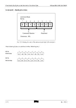
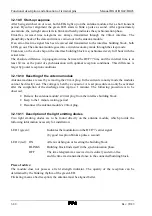
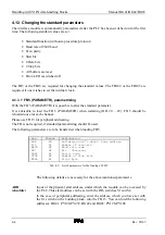
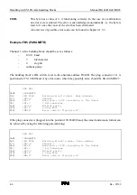
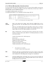
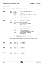
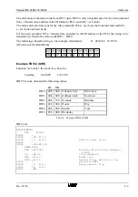
The data words of the data block DB99 are allocated as follows:
DW0
DL0:
40h
=
building block’s aknowledgement byte
DR0: Error byte
00h
=
no error
01h
=
building block wrongly addressed or defect
04h
=
data block not available
0Ah
=
wrong clock command
DW1
DL1:
40h
=
clock should be addressed
DR1:
Sub-command for operating clock
01h
=
Transfer time and date to PLC
(BCD depiction)
02h
=
irrelevant if using the DCF77
03h
=
irrelevant if using the DCF77
04h
=
irrelevant if using the DCF77
05h
=
Transfer time and date to PLC
(ASCII character)
DW1 is to be previously occupied by the user prior to the loading of FBs.
DW2
DL2
00h…59h
seconds (BCD)
DR2
00h…59h
minutes (BCD)
DW3
DL3
00h…23h
hours (BCD)
DR3
01h…31h
day (BCD)
DW4
DL4
01h…12h
month (BCD)
DR4
00h…99h
year (BCD)
DW5
DL5
00h…06h
weekday, Sunday = 00h (BCD)
DR5
00h
Summary of Contents for SSM-BG41
Page 2: ...Lerrzeichen...
Page 8: ...Contents Manual BG41 BG42 BG43 iv Rev 99 49...
Page 10: ......
Page 16: ......
Page 26: ...Firmware s memory distribution Manual BG41 BG42 BG43 2 10 Rev 99 49...
Page 28: ......
Page 53: ...Manual BG41 BG42 BG43 Interface modules Rev 99 49 3 25 3 2 7 2 Data flow Fig 3 26 Data flow...
Page 114: ...Functional description and allocation of terminal pins Manual BG41 BG42 BG43 3 86 Rev 99 49...
Page 116: ......
Page 215: ...Manual BG41 BG42 BG43 Software Rev 99 49 4 99 Month 06h Year 95h Weekday Tuesday 02h...
Page 222: ...Application of interfaces without data handling blocks Manual BG41 BG42 BG43 4 106 Rev 99 49...
Page 224: ......
Page 258: ...Structure guidelines Manual BG41 BG42 BG43 5 34 Rev 99 49...
Page 260: ......
Page 274: ...Overview cycle load Manual BG41 BG42 BG43 6 14 Rev 99 49...
Page 275: ...Appendix A List of figures A 1 B Index of tables B 1 C Index C 1...
Page 276: ......
Page 280: ...List of figures Manual BG41 BG42 BG43 A 4 Rev 99 49...

