background image

Manual BG41/BG42/BG43

Interface modules

Rev. 99/49

3-47

3.2.9 Analogue input (MD40-44) and output module (MD45-49)

3.2.9.1 General

The module for analogue input or analogue output enables the connection of analogue process
interface equipment to the AG-115U, -135U and -155U. They convert the analogue signals with a
resolution of 12 bits into a SPS-CPU digital signal and vice versa. The individual channels are
polled and when requested by the SPS are directly transfered without delay. The interface’s digital
control is electrically decoupled.

The use of analogue modules will be supported from interface building block firmware number
4118V14 on.

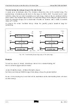
The analogue input module possesses 8 inputs, the analogue output module 4 outputs. When using
the module on a SSM-BG43, up to 12 output channels or 24 input channels are available. With a
scanning period of 1 ms per channel, a maximum scanning period of

8 ms is produced by 8 inputs, if all channels are polled.

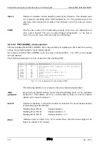
Fig. 3-37: Structure of the analogue input module

With the analogue output module, an undefined current is issued during the
running up!

The following modules are presently available:

=

MD40

Voltage input 8 channels, single ended, 12 bit, ±10V

=

MD41

Voltage input 8 channels, single ended, 12 bit, ±5V or 0...10V

=

MD42

Voltage input 8 channels, single ended, 12 bit, 0...5V

=

MD43

Voltage input 8 channels, single ended, 12 bit, 0...20 or 4...20mA

=

MD44

Connection from PT100, 4 channel temperature area: -200°C...850°C

=

MD45

Voltage output 4 channels, 12 bit, ±10V

=

MD46

Voltage output 4 channels, 12 bit, ±5V

=

MD47

Voltage output 4 channels, 12 bit, 0...10V

=

MD48

Voltage output 4 channels, 12 bit, 0...5V

=

MD49

Current output 4 channels, 12 bit 0...20 or 4...20 mA

Summary of Contents for SSM-BG41

Page 1: ...Subject to change to cater for technical progress Manual SSM BG41 BG42 BG43 Order No VIPA SSM HB29E Rev 99 49...

Page 2: ...Lerrzeichen...

Page 3: ...will result in liability for damages Copyright 2000 VIPA Gesellschaft f r Visualisierung und Proze automatisierung mbH Ohmstra e 4 D 91074 Herzogenaurach Phone 49 9132 744 0 Fax 49 9132 744 144 EMail...

Page 4: ...description to the structure mode of operation and allocation of pins The use with or without data handling blocks will be described for the module SSI counter analogue input output and DCF77 Chapter...

Page 5: ...backplane connector 2 8 2 3 1 Backplane connector X1 2 8 2 3 2 Backplane connector X2 2 8 2 4 Block diagram of firmware 2 9 2 5 Firmware s memory distribution 2 9 3 INTERFACE MODULES 3 1 3 1 General...

Page 6: ...1 5 1 Startup procedure 5 1 5 2 Presetting 5 2 5 2 1 Mounting place in PLC 115U 5 2 5 2 2 Mounting places in PLC 135U 5 3 5 2 3 Mounting place in PLC 150U 5 4 5 2 4 Mounting place in PLC 155U 5 5 5 2...

Page 7: ...RS232C module 6 3 6 2 4 RS422 RS485 module 6 4 6 2 5 RS422P RS485P module 6 4 6 2 6 CENTRONICS module 6 5 6 2 7 SSI module 6 5 6 2 8 Counter module 5V 24V 6 6 6 2 9 Analogue input module 6 7 6 2 10 A...

Page 8: ...Contents Manual BG41 BG42 BG43 iv Rev 99 49...

Page 9: ...1 1 Handling electrostatically sensitive modules 1 1 1 1 2 Shipping electrostatically sensitive modules 1 2 1 1 3 Tests and modifications to electrostatically sensitive modules 1 2 1 2 General 1 3 1 3...

Page 10: ......

Page 11: ...ed by energies or voltage which lie far below the human s point of perception If a person who is not electrically discharged handles building blocks liable to electrostatic danger such voltages may oc...

Page 12: ...battery s connections are not touched or short circuited when dispatched in conductive packaging 1 1 3 Tests and modifications to electrostatically sensitive modules The following aspects are to be o...

Page 13: ...loyment The VIPA interface building block is used in PLC systems as an interface for the input and output of data It is equipped with transmitting and receiving buffers each with 256 bytes which are r...

Page 14: ...M MD22 RS422 RS485 Module non floating Order No VIPA SSM MD21 RS422P Module floating Order No VIPA SSM MD33 RS485P Module floating Order No VIPA SSM MD34 CENTRONICS Module Order No VIPA SSM MD24 5V Co...

Page 15: ...ture 2 2 2 2 1 Building block BG41 2 2 2 2 2 Building block BG42 2 4 2 2 3 Building block BG43 2 6 2 3 Allocation of the backplane connector 2 8 2 3 1 Backplane connector X1 2 8 2 3 2 Backplane connec...

Page 16: ......

Page 17: ...a channel from the PLC is recorded by the building block in the appropriate transmission buffer 256 Byte and from there is sent through the interface In the other direction Interface PLC the data rece...

Page 18: ...lding block BG41 has 1 interface which can be adapted to certain physical modes of transmission by means of interface modules The front panel of the module consists of 1 A 25 pole SubD socket for the...

Page 19: ...Manual BG41 BG42 BG43 Interface building blocks Rev 99 49 2 3 Fig 2 3 Position of jumpers and DIL switches on BG41...

Page 20: ...2 interfaces which could be adapted to certain physical modes of transmission by means of interface modules The front panel of the module consists of 1 Two 25 pole SubD socket for the two interfaces...

Page 21: ...Manual BG41 BG42 BG43 Interface building blocks Rev 99 49 2 5 Fig 2 5 Position of Jumpers and DIL switches on BG42...

Page 22: ...interfaces which could be adapted to certain physical modes of transmission by means of interface modules The front panel of the module consists of 1 Three 25 pole SubD socket for the three interfaces...

Page 23: ...Manual BG41 BG42 BG43 Interface building blocks Rev 99 49 2 7 Fig 2 7 Position of jumpers and DIL switches on BG43...

Page 24: ...c ADB06 DB2 20 n c ADB07 DB3 22 n c ADB08 DB4 24 n c ADB09 DB5 26 n c ADB10 DB6 28 n c ADB11 DB7 30 24V BASP M24V 32 BASPA M n c Tab 2 1 Allocation of the backplane connector X1 2 3 2 Backplane connec...

Page 25: ...irmware Fig 2 8 Firmware block diagram BG43 2 5 Firmware s memory distribution The Z80 processor on communication processors has an address range of 64 KByte This is distributed as follows 0000 7FFF F...

Page 26: ...Firmware s memory distribution Manual BG41 BG42 BG43 2 10 Rev 99 49...

Page 27: ...l pins 3 4 3 2 1 20mA current loop modul MD25 3 4 3 2 2 RS232C module MD22 3 9 3 2 3 20mA current loop RS232C combination module MD26 3 12 3 2 4 RS422 RS485 module MD21 3 14 3 2 5 RS422P MD33 and RS48...

Page 28: ......

Page 29: ...onnection with keyboards terminals or printers Time and clock acquisition Recording the time standard of PTB Braunschweig Recording and output of analogue process quantities 3 1 1 Voltage supply 5V an...

Page 30: ...e of Module Order LED No 1 2 3 4 20mA Current Loop MD25 red receive red send 20mA Current Loop RS232C Combination MD26 red receive red send RS232C MD22 green receive green send RS422 RS485 MD21 yellow...

Page 31: ...D21 MD22 MD25 MD26 MD33 MD34 FB20 FB27 FB21 26 1 Mettler Balance MD22 MD25 MD26 FB17 FB18 FB7 FB8 Hohner Encoder MD34 FB5 FB19 Parallel functions MD24 FB100 FB101 FB5 FB3 Additional functions SSI modu...

Page 32: ...nt or bus connections can be realised with the 20mA current loop module The module contains two line current loops for transmission and reception In bus operations the module in a voltage free state c...

Page 33: ...A current loop module the interface can be operated as a passive or active part of the transmission link The type of contacts for peripheral equipment varies accordingly It is possible to obtain 24 V...

Page 34: ...active part of a current loop they can be supplied internally or externally from the 20mA current sources found on the module internally through the back plane bus base plug X1 or X2 externally throu...

Page 35: ...e part of the transmission link the peripheral device as the passive part Fig 3 4 An active 20mA current loop interface Observe shielding See construction guidelines in chapter 5 The jumpers J6 on the...

Page 36: ...terface Peripheral equipment e g the printer PT 88 as the active part are in the position to take over the supply of the 20mA connection In this manner the serial interface can be operated as the pass...

Page 37: ...n occurs by data signal and control lines The RS232C module serves the point to point connection on the basis of the RS232C standards No presetting has to be observed when operating the RS232C interfa...

Page 38: ...232C interface a hardware handshake is used through the signals RTS and CTS These handshake signals must be operated by peripheral equipment If the employed peripheral equipment is operated with a DTR...

Page 39: ...this case according to VIPA the RTS CTS should always be bridged With this type of connection it must be insured that no character is lost This can be achieved by observing the following points a low...

Page 40: ...e internal voltage supply is carried out by the back plane bus If the external voltage supply 25 pole SubD sockets is switched to the 20mA current source the plug connectors X3 and X5 must be replugge...

Page 41: ...al pins when using a 20mA Current Loop Module 3 2 3 3 Allocation of terminal pins when using a RS232C module Details on the RS232C module are to be found in chapter 3 2 2 Fig 3 12 Allocation of termin...

Page 42: ...to 16 suscribers The RS485 interface was developed in order to enable a higher number of bus suscribers to be connected to the bus operation Up to 32 suscribors can in this case be connected Similar t...

Page 43: ...3 15 3 2 4 2 Allocation of the RS422 RS485 module s terminal pins Fig 3 14 Allocation of terminal pins when using a RS422 RS485 moduls It is possible to obtain 24 V from pin 11 24 V and pin 22 ground...

Page 44: ...to point connection with a RS422 RS485 module Two twisted pair wires which have to be particularly shielded are to be used for the TX and RX links A load resistance of 100 can be switched between the...

Page 45: ...nection The RS485 interface uses the two wire connection Due to the links the sent data is immediately recoupled The recoupled data is to be filtered by using software It is advisable to use the RS485...

Page 46: ...should be selected if several external pieces of equipment are to be connected to the interface as receivers Fig 3 17 Multidrop connection with a RS422 RS485 module The number of connection possibili...

Page 47: ...our wire connection should be selected if several external pieces of equipment are to be connected to the bus Fig 3 18 Four wire connection with a RS422 RS485 module The number of slave connections de...

Page 48: ...S422P or RS485P modules on the bus ends a 100 terminating resistor is additionally connected by means of the existing switch on the module The terminating resistor is connected when the switch is in t...

Page 49: ...Bus Connection By linking Rx and Tx or Rx and Tx it is possible to produce a two wire bus connection The RS485 interface uses the two wire connection Due to the links the sent data is immediately rec...

Page 50: ...49 3 2 6 CENTRONICS module MD24 3 2 6 1 General The module is used for controlling equipment with CENTRONICS interfaces The module is preferably used for controlling printers When using the CENTRONIC...

Page 51: ...rminal pins when using a CENTRONICS module Fig 3 24 Point to point connection when using a CENTRONICS module The allocation of the 25 pole SubD sockets corresponds to the allocation selected by IBM fo...

Page 52: ...the interface module and consequently the control Connections for 2 test probes are available on the module The connected test probes can be supplied directly by the module and therefore do not requir...

Page 53: ...Manual BG41 BG42 BG43 Interface modules Rev 99 49 3 25 3 2 7 2 Data flow Fig 3 26 Data flow...

Page 54: ...suitable cable length The clock frequency was increased to 10 MHz with the release 4 The cable length depends on the clock frequency and the transfer rate Cable length for 10 MHz Interface modules ma...

Page 55: ...S485 driver software In principle 24 bit data is received If an encoder with a higher data width is used as for example 25 bits the least significant bit LSB is therefore cut off The test probes can b...

Page 56: ...Building block s periphery address K EI KY Number of channels Number of encoders WER1 W Output value low word WER2 W Output value high word PAFE BY Error byte Tab 3 4 List of parameters for the loadi...

Page 57: ...eripheral address of the block PY128 in accordance with F080h KANR KF 1 Channel 1 on the interface building block PROC KF 12 SSI procedure code 12 FEHL MB 199 Error code in flag byte 199 OB22 SPA FB 1...

Page 58: ...ation of the interface without Data Handling Blocks can be found in chapter 4 2 Select the SSI function for the corresponding interface channel via the parameter channel with the command 5 Fig 3 29 Fu...

Page 59: ...ty of selecting 2 SSI encoders 0 Encoder 1 1 Encoder 2 Fig 3 30 Reading of an SSI encoder with command 1 The following bytes are returned to the data channel as follows Bit No 7 6 5 4 3 2 1 0 LSB D7 D...

Page 60: ...it 3 in byte 1 is used as the control bit for the block commands If this bit is set at 1 the command applies for all connected sonsors of the channel The mode bits are occupied as follows Bit 0 to 4 W...

Page 61: ...er 1 and counter 2 are to be cascaded the jumpers X1 and X2 are to be replugged into position 32 With the plug connectors from X4 to X6 one can alternatively place Carry or Borrow with each counter on...

Page 62: ...A carry which is set is deleted by a borrow and vice versa The carry or borrow flag can be alternatively placed on the yellow light emitting diodes on the front of the building block and on the 25 po...

Page 63: ...or 3 active high max 5V 100mA inactive high impedance UAxa Counter input 1 or 2 for counter 1 2 or 3 active low TTL or RS 422 level UAxa Counter input 1 or 2 for counter 1 2 or 3 active high only conn...

Page 64: ...put 5V Supply voltage output 24V Supply voltage output for external voltage supply or extraction M24 Supply voltage output by adjustment to internal voltage supply CYa BWa Carry or borrow output of co...

Page 65: ...ter 3 2 8 8 Programming the counter modules If the counter module is to be used for one or more interfaces of the building blocks BG41 BG42 or BG43 the counter procedure is to be set with FB 100 or FB...

Page 66: ...filed in a data word the corresponding data block must be opened before loading FB 10 with A DBxx The following details are necessary for the abovementioned parameters ADR Input of the physical start...

Page 67: ...word the correspponding data block must be opened before loading FB 11 with A DBxx The following details are necessary for the abovementioned parameters ADR Input of the physical start address under...

Page 68: ...unter 1 0 7 MOD2 KF Mode for counter 2 0 7 MOD3 KF Mode for counter 3 0 7 Tab 3 7 List of parameters for the loading of FB12 The following details are necessary for the abovementioned parameters ADR I...

Page 69: ...wards UA2x ground UA2x ground Mode 1 5 Direction discriminator With this mode out of phase input pulses e g from a rotary pulse generator can be evaluated Depending on the phase position of UA1 to UA2...

Page 70: ...quency is to be positioned at input UA1 and a known frequency e g created by the clock generator at UA2 If UA2 goes from 1 to 0 the counting process starts with the frequency of UA1 If UA2 goes from 0...

Page 71: ...nnel number MOD1 KF 1 Counter 1 in mode 1 MOD2 KF 3 Counter 2 in mode 3 MOD3 KF 0 Counter 3 in mode 0 00020 BE Cycle OB OB1 00002 SPA FB 10 Read counter value NAME LESEN ADR KH F080 Base address KNR K...

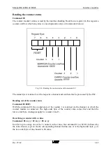
Page 72: ...ccupies the high order byte yy occupies the low order byte The two bytes are structured as follows Fig 3 35 Counter s sequence bytes from command 80 Byte xx Bit 7 RESET 0 all counters activated 1 all...

Page 73: ...y the PLC Reading out of the counter state Command 01 02 03 With the command 01 the counter state of the counter 1 is returned via the channel to which the counter module is connected The high order b...

Page 74: ...nter reading should be read The following bytes are to be transferred a b From the building block 6 bytes can be read through the corresponding channel whereby the counter s high order byte is always...

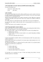
Page 75: ...using the module on a SSM BG43 up to 12 output channels or 24 input channels are available With a scanning period of 1 ms per channel a maximum scanning period of 8 ms is produced by 8 inputs if all...

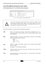
Page 76: ...Functional description and allocation of terminal pins Manual BG41 BG42 BG43 3 48 Rev 99 49 3 2 9 2 Data flow Fig 3 38 Data flow of analogue input or analogue output module...

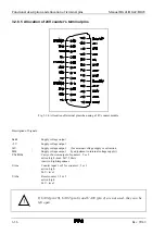
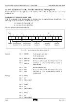
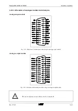
Page 77: ...f analogue module s terminal pins Analogue input module Fig 3 39 Allocation of terminal pins when using an analogue input module Analogue output module Fig 3 40 Allocation of terminal pins when using...

Page 78: ...ation of terminal pins Manual BG41 BG42 BG43 3 50 Rev 99 49 3 2 9 4 Functional mode Analogue input module Fig 3 41 Block diagram of an analogue input module Analogue output module Fig 3 42 Block diagr...

Page 79: ...e following parameters are to be transferred when loading FB 50 Des Format Explanation ADR KF Peripheral base address of the building block KANR KF Number of channels MODL KF Module number NKAN KF Max...

Page 80: ...tart or restart OB 20 22 Fb51 is to be loaded for each channel The following parameters are to be transferred when loading FB51 Des Format Explanation ADR KF Peripheral base address of the building bl...

Page 81: ...ransferred when loading FB52 Des Format Explanation ADR KF Peripheral base address of the building block K EI KY Number of channels analogue input WERT W Output value FEHL BY Error byte Tab 3 10 List...

Page 82: ...her Input of the peripheral address under which the building block can be controlled by the PLC This address can be set with the DIL switches S1 and S2 Further details can be found in chapter 5 K OU K...

Page 83: ...ters ADR peripher Input of the peripheral address under which the building block can be controlled by the PLC This address can be set with the DIL switches S1 and S2 Further details can be found in ch...

Page 84: ...dth of maximal 2 Byte 215 32768 To preserve the sensor resolution always choose the possibly greatest numerical range for normalizing effective range of the sensor 5V 10V 5V 10V nominal range 2048 204...

Page 85: ...e peripheral address under which the building block can be controlled by the PLC This address can be set with the DIL switches S1 and S2 Further details can be found in chapter 5 K EI K Number of chan...

Page 86: ...owing details are necessary for the abovementioned parameters ADR absolut Input of the peripheral address under which the building block can be controlled by the PLC This address can be set with the D...

Page 87: ...eripheral address under which the building block can be controlled by the PLC This address can be set with the DIL switches S1 and S2 Further details can be found in chapter 5 K EI K Number of channel...

Page 88: ...ementioned parameters ADR peripher Input of the peripheral address under which the building block can be controlled by the PLC This address can be set with the DIL switches S1 and S2 Further details c...

Page 89: ...er of the module INOU KF 1 Analogue input number 1 MODE KM 00000000 00000010 Signed normalised depiction in mV no limit OFFS KF 0 Offset of I O FEHL MB 55 Error code to be filed in MB 55 SPA FB 59 Tim...

Page 90: ...nnel number number of the input channel WERT MW 20 Flag word MW20 for the analogue input value FEHL MB 55 Error code to be filed in MB55 A DB20 Open data block DB20 SPA FB 58 NAME IN_DW ADR KF 128 Bas...

Page 91: ...Returning of the status bits FEHL MB 18 Error byte If the min or max value falls down or up a corresponding status bit is set SPB FB 56 NAME MIN MAX ADR KF 128 Base address of the SSM PY128 K OU KY 1...

Page 92: ...nd in chapter 4 2 Select the procedure with command 5 Fig 3 44 Function selection of analogue input analogue output with command 5 3 2 9 6 2 Commands for the data channel Use the data channel for tran...

Page 93: ...analogue input output with command 1 The line 0 7 is assigned to the inputs or outputs The following bytes are returned as follows Bit No 7 6 5 4 3 2 1 0 LSB D7 D6 D5 D4 D3 D2 D1 D0 Bit No 7 6 5 4 3...

Page 94: ...al BG41 BG42 BG43 3 66 Rev 99 49 Command 2 Writing the analogue value Fig 3 46 Writing the analogue value of the analogue input output with command 2 Bit 3 is used as the control bit for block command...

Page 95: ...ock commands If this bit is set at one this command applies to all lines Offset The offset carries out a zero balance 11 bits signed D11 Sign The mode bits are occupied as follows Bit 7 is not defined...

Page 96: ...command Fig 3 48 Module selection of the analogue input output with command 4 Line 0 2 Determines the number of lines to be polled Module Number The module number corresponds to the last numeral of t...

Page 97: ...Manual BG41 BG42 BG43 Interface modules Rev 99 49 3 69 Command 5 Scaling With scaling four extra bytes are transferred as an argument Fig 3 49 Scaling of an analogue input output with command 5...

Page 98: ...99 49 Command 6 Reading the status Fig 3 50 Reading the status of the analogue input output with command 6 The following bytes are sent back in the following way Bit No 7 6 5 4 3 2 1 0 MIN Status E7...

Page 99: ...es Rev 99 49 3 71 Command 7 Writing of the MIN MAX limits Fig 3 51 MIN MAX levels of the analogue input output with command 6 Bit 3 is used as the control bit for block commands If this bit is set at...

Page 100: ...rs with the AG 115U 135U and 155U The modul delivers a 16 Bit integer value proportional to the temperature sensor s resistor This value is definitely assigned to the sensor s temperature When using t...

Page 101: ...Manual BG41 BG42 BG43 Interface modules Rev 99 49 3 73 3 2 9 7 3 Connection example Fig 3 54 An application example of the temperature module...

Page 102: ...nal to a 20mA interface Every 20mA interface can be used as a communication module for example the SSM MD25 and the SSM MD26 modules Every full hour the antenna module synchronizes with the quartz clo...

Page 103: ...nstitute for Physical Technology Braunschweig is located in Mainflingen near Frankfurt Like a radio the reception is greatly dependent upon place and location However within a radius of 1500 km around...

Page 104: ...Functional description and allocation of terminal pins Manual BG41 BG42 BG43 3 76 Rev 99 49 3 2 10 3 The module s dimensions Fig 3 57 The dimensions of the DCF77 antenna module...

Page 105: ...ime plan The following figure shows the temporal course of transmtting the coded time information from the German time signal transmitter Fig 3 59 Plan of the coded time information The carrier freque...

Page 106: ...49 3 2 10 6 Transmission protocol The antenna module sends 7 bytes through the 20mA Current Loop interface The bytes are not acknowledged The following is for example transferred 06 06 95 14 53 00 Ide...

Page 107: ...10 7 Alignment of the antenna As shown in Fig 3 60 the antenna must be aligned so that it is tangential to the transmitter Fig 3 60 Alignment of the DCF77 antenna module 3 2 10 8 Connection example F...

Page 108: ...ion conditions 3 2 10 10 Resetting of the antenna module Antenna modules are reset by removing the 20 mA plug In the current economy mode the modules can not be directly reset The voltage is held by a...

Page 109: ...an interface module will be described below step by step Connect the 20mA module to the interface building block Jumper J11 on the interface building block in position 75 19200Baud Plug the 24V suppl...

Page 110: ...the following chapters FB100 see chapter 4 1 4 1 FB5 see chapter 4 1 3 1 Example The following example shows how an interface building block is to be parametrized so that one can read the time signal...

Page 111: ...ss can be set with the DIL switches S1 and S2 In the case of peripheral addressing enter the address which you have set with the DIL switch S1 on the building block into FB103 The following addresses...

Page 112: ...mand DW1 DL1 40h clock should be addressed DR1 Sub command for operating clock 01h Transfer time and date to PLC BCD depiction 02h irrelevant if using the DCF77 03h irrelevant if using the DCF77 04h i...

Page 113: ...e FB102 UHR Function set clock the clock is to be set to Tuesday 06 06 89 14 53 00 DB 99 is to be allocated the following values DL DR DW0 40h 00h Acknow byte Error byte DW1 40h 02h Address clock Set...

Page 114: ...Functional description and allocation of terminal pins Manual BG41 BG42 BG43 3 86 Rev 99 49...

Page 115: ...andling without a protocol and procedure 4 12 4 1 6 Data handling with procedure STX ETX 4 18 4 1 7 Handling with procedure 3964 R 4 20 4 1 8 Handling with prozedure 3964 R with RK512 4 41 4 2 Applica...

Page 116: ......

Page 117: ...40 FB43 FB44 3964 R procedure MD21 MD22 MD25 MD26 MD33 MD34 FB30 FB37 FB31 33 3964 R with RK 512 procedure MD21 MD22 MD25 MD26 MD33 MD34 FB20 FB27 FB21 26 1 Mettler Balance MD22 MD25 MD26 FB17 FB18 FB...

Page 118: ...ed Further information on the methods of addressing can be found in chapter 5 4 1 2 Overview of parameterizing possibilities Parameterizing with VIPA data handling blocks Changing of the standard para...

Page 119: ...ata passively received FB22 SEND ALL Requested data sent Data Handling Blocks dependant on the Module CENTRONICS module FB3 SEND Data output without a procedure but with absolute addressing FB13 SEND...

Page 120: ...ng OB 20 22 FB 5 should be reloaded once for each channel Please use FB 15 for peripheral addressing The FB is not required if standard parametrizing should be used The following parameters are to be...

Page 121: ...aud rates can be set by entering the respective codes Optional baud rates from 150 to 38400 baud can be set with the plug connector J11 on the building block To enable this J11 which is inserted in it...

Page 122: ...The plug connector J 11 is positioned at 75 19200 baud Any error codes which may possibly arise should be filed in MB127 SPA FB5 NAME PARAMETR ADR KH F0A0 Building block s absol base address K 0 KY1...

Page 123: ...t with the DIL switch S1 on the building block into FB103 The following addresses can be loaded BG41 PY128 PY252 BG42 and BG43 PY128 PY248 DB Entry of the data blocks in which the data record for sett...

Page 124: ...Transfer time and date to PLC BCD depiction 02h Set clock Sub command in DW2 up to DW5 03h Set clock one hour forward adjusts from winter to summer time 04h Set clock one hour back adjusts from summer...

Page 125: ...ted Fr 02 06 89 22 55 58 Allocation of the Data Blocks Example FB102 UHR Function set clock the clock is to be set to Tuesday 06 06 89 14 53 00 DB 99 is to be allocated the following values DL DR DW0...

Page 126: ...L switch S1 onto the building block into FB101 The following addresses can be loaded BG41 PY128 PY252 BG42 and BG43 PY128 PY248 KANR KANR Number of channels through which the data is to be transmitted...

Page 127: ...F0A0 Building block s absolute base address KANR KF 1 Channel 1 PROC KF 0 Code for without protocol procedure FEHL MB127 Error code in flag byte 127 Procedure STX ETX should be used through channel 3...

Page 128: ...tart flag Tab 4 6 List of parameters for the loading of FB3 The following details are necessary for the abovementioned parameters ADR Input of the physical start address under which the building block...

Page 129: ...continued Example FB3 SEND 31 bytes should be transmitted through channel 1 which are filed from data word DW5 in DB 23 The DIL switches are set to the absolute address F1A0h and the M4 7 is used as t...

Page 130: ...witch S1 on the building block into FB14 The following addresses can be loaded BG41 PY128 PY252 BG42 and BG43 PY128 PY248 K DB K Number of channels through which the data should be received This chann...

Page 131: ...s the bit is at the signal state 1 the handling of the function block is discontinued Management of write and read pointers The handling of write and read pointers can be clarified by using two exampl...

Page 132: ...every byte calculated from the new starting point and the read pointer is updated accordingly Fig 4 1 Evaluation possibility 1 with the help of write and read pointers Example 2 Write and read pointer...

Page 133: ...e the data is to be filed SPA FB 4 NAME RECEIVE ADR KH F180 Absolute base address K DB KY1 100 Channel 1 data block 100 SZ MB10 LZ MB11 ANF MW12 ANZ MB14 FEHL MB20 Error code in flag byte 20 NEUS M 1...

Page 134: ...B 44 come together with the PLC 4 1 6 1 FB40 PARA_STX parametrizing of the STX ETX procedure With FB40 the function for reparametrizing the STX ETX procedure is selected The following parameters are t...

Page 135: ...places the FB3 The list of parameters is identical to those of the FB3 The description of FB3 can be found in chapter 4 1 5 1 4 1 6 3 FB44 RECEIVE data reception with STX ETX procedure This data handl...

Page 136: ...to be able to work with procedure 3964 or 3964R the following VIPA data handling blocks have been made available SYNCHRON FB37 from firmware level 401xV50 and all 4118 With this function block the bu...

Page 137: ...ual BG41 BG42 BG43 Software Rev 99 49 4 21 4 1 7 2 Procedure The following describes the structure of the procedure and the telegrams Fig 4 3 Procedure 3964 R You can transmit max 250 bytes per telegr...

Page 138: ...3 BAUD KF Baud rate code 1 11 10 9600Baud FORM KM Transmission format 8bit even parity 2 stop PRIO KF 0 low 1 high priority BLOC KF Block size in bytes always even numbered ZVZ KF Character delay tim...

Page 139: ...the PLC and the interface building block every time the data handling blocks SEND and RECEIVE are loaded The greater the number of bytes to be exchanged the higher the cycle time load The block size...

Page 140: ...Invalid clock data Interface building block 7 Parametrizing wrong Interface building block 8 Wrong number of parameters Interface building block 9 Not used 10 Not used 11 Invalid value on the operand...

Page 141: ...5535 Example FB37 SYNCHRON SPA FB37 NAME SYNCHRON ADRE KH F080 Building block s address as set by DIL switches SSNR KF 1 Interface number 1 2 3 BAUD KF 10 Baud rate code 1 11 10 9600baud FORM KM 00000...

Page 142: ...ss set by DIL switches SSNR KF Interface number 1 2 3 BAUD KF Baud rate code 1 11 10 9600baud FORM KM Transmission format 8bit even parity 2 stop PRIO KF 0 low 1 high priority BLOC KF Block size in by...

Page 143: ...handling blocks SEND and RECEIVE are loaded The greater the number of bytes to be exchanged the greater the cycle time load The block size has no influence on the data transmission The building block...

Page 144: ...number of parameters Interface building block 9 Not used 10 Not used 11 Invalid value on operands ADRE Data handling block 12 Invalid value on operands SSNR Data handling block 13 Invalid value on ope...

Page 145: ...ock s address as set by DIL switches SSNR KF 1 Interface number 1 2 3 BAUD KF 10 Baud rate code 1 11 10 9600baud FORM KM 00000001 11111100 Transmission format 8bit even parity 2 stop PRIO KF 0 0 low 1...

Page 146: ...Interface number 1 2 3 A NR KF Order number 1 255 ZTYP KC Details of data type DBNR KY Number of data blocks detailed under target type of given function block BWNR KY Byte word number from which an i...

Page 147: ...ight byte Valid area 2 255 If this area is violated it results in PAFE 17 If the given DB does not exist the data handling block will therefore register PAFE 19 BWNR Byte word number By means of these...

Page 148: ...ta block from the interface building block it places as an identifier for job running bit 1 in the right byte of the display word If all data blocks have been correctly imported from the interface bui...

Page 149: ...DB too short by indirect parametrizing 21 Invalid target type ZTYP 23 Target area too short BWNR MXBW 26 Invalid order number 31 Invalid number of valid data at reception MXBW NEUS As long as the bit...

Page 150: ...rametrized on the operand ZTYP This is the identifier for indirect parametrizing The DB number in which the operands lie are to given on the operand DBNR The data word number from where the operands l...

Page 151: ...ess set with DIL switches SSNR KF Interface number 1 2 3 A NR KF Order number 1 255 QTYP KC Source type QDBN KY DB no by source type DB or DX QBWN KY Byte word number form where data is to be sent BWA...

Page 152: ...ror message PAFE 27 QDBN If the source type DB or DX are selected the DB no is to be given into the right byte Valid area 2 255 If this area is violated a PAFE 28 is registered If the given DB or DX d...

Page 153: ...placed in the right byte of the display word as identifier for job running If all data blocks have correctly been received by the interface building block and the receiver does not report an error the...

Page 154: ...parametrizing DBNR 20 DB too short by indirect parametrizing 26 Invalid order number A NR 27 Invalid source type QTYP 28 Invalid source DB number QDBN 29 Source DB not available 31 Invalid amount of v...

Page 155: ...the operand QTYP This is the identifier for indirect parametrizing The DB number in which the operands lie is to be given on the operands QDBN The DB s data word number from where the operands lie mus...

Page 156: ...on ADRE KH The address set with DIL switches NEUS BI New start bit PAFE BY Error messages or parametrizing are filed in this byte Tab 4 14 List of parameters for loading FB28 The following details are...

Page 157: ...with the procedure 3964 or 3964R called 3964 R in the following with the RK512 protocol the following VIPA data handling blocks have been made available SYNCHRON FB27 from firmware level 401xV50 and...

Page 158: ...equipment SEND ALL FB22 From this function block requested telegrams from the partner equipment are answered Depending on the case of application only one function block is always required from the gr...

Page 159: ...E as well as between BCC and DLE ZVZ is monitored during the entire reception of the telegrams STX is transmitted again when QVZ is expired to STX After 5 attempts a NAK is sent and the connection set...

Page 160: ...s attached to the end of the telegram for better data protection The BCC byte is formed by an XOR linkage through the data of the entire telegram including the DLE ETX When a BBC byte is received whic...

Page 161: ...legram sequence SEND Transmission of data Fig 4 5 SEND of the procedure 3964 R with RK512 FETCH Fetching data Fig 4 6 FETCH of the procedure 3964 R with RK512 The procedure waits in both cases a maxim...

Page 162: ...put telegram Each telegram has a header Depending on the history of the telegram traffic the header contains all necessary information Fig 4 7 Structure of an output telegram from 3964 R with RK512 By...

Page 163: ...Manual BG41 BG42 BG43 Software Rev 99 49 4 47 Example Output telegram Fig 4 9 Example of an output...

Page 164: ...blocks Manual BG41 BG42 BG43 4 48 Rev 99 49 Structure of an input telegram Fig 4 10 Structure of a normal input telegram By data amounts 128 Bytes sequence telegrams are transmitted Fig 4 11 Structur...

Page 165: ...Manual BG41 BG42 BG43 Software Rev 99 49 4 49 Example Input telegram Fig 4 12 Example of an input telegram...

Page 166: ...ceived This occurs both by input and output commands If the coordination flag is set and a telegram with this flag has been received the data is not accepted or passed on but an error response message...

Page 167: ...AUD KF Baud rate code 1 11 10 9600baud FORM KM Transmission format 8bit even parity 2 stop PRIO KF 0 low 1 high Priority BLOC KF Block size in bytes always even numbered ZVZ KF Character delay time Va...

Page 168: ...nterface building block every time the data handling blocks SEND SEND ALL RECEIVE RECEIVE ALL FETCH are loaded The greater the number of bytes to be exchanged the greater the cycle time load The block...

Page 169: ...ng Interface building block 8 Wrong number of parameters Interface building block 9 Not used 10 Not used 11 Invalid value on the operands ADRE Data handling block 12 Invalid value on the operands SSNR...

Page 170: ...ed ZVZ 1 65535 QVZ 1 65535 Example FB27 SYNCHRON SPA FB27 NAME SYNCHRON ADRE KH F080 The address set with DIL switches SSNR KF 1 Interface number 1 2 3 BAUD KF 10 Baud rate code 1 11 10 9600baud FORM...

Page 171: ...ith DIL switches SSNR KF Interface number 1 2 3 BAUD KF Baud rate code 1 11 10 9600baud FORM KM Transmission format 8bit even parity 2 stop PRIO KF 0 low 1 high priority BLOC KF Block size in bytes al...

Page 172: ...to be exchanged between the PLC and the interface building block every time the data handling blocks SEND SEND ALL RECEIVE RECEIVE ALL FETCH are loaded The greater the number of bytes to be exchanged...

Page 173: ...Wrong parametrizing Interface building block 8 Wrong number of parameters Interface building block 9 Not used 10 Not used 11 Invalid value on the operands ADRE Data handling block 12 Invalid value on...

Page 174: ...80 Building block s address as set with DIL switches SSNR KF 1 Interface number 1 2 3 BAUD KF 10 Baud rate code 1 11 10 9600baud FORM KM 00000001 11111100 Transmission format 8bit even parity 2 stop P...

Page 175: ...number 1 255 ZTYP KC Function block details DBNR KY Number of handling blocks detailed under the target type of the given function block BWNR KY Byte word number from where an incoming telegram is to...

Page 176: ...lected the DBNR is to be entered in the right byte Valid area 2 255 If this area is violated it results in PAFE 17 If the given DB does not exist the data handling block will therefore register a PAFE...

Page 177: ...k from the interface building block it places as an identifier for job running bit 1 in the right byte of the display word If all data blocks have been correctly imported from the interface building b...

Page 178: ...able DBNR 20 DB too short by indirect parametrizing 21 Invalid target type ZTYP 23 Target area too short BWNR MXBW 26 Invalid order number 31 Invalid amount of valid data at reception MXBW NEUS As lon...

Page 179: ...on the operand ZTYP This is the identifier for indirect parametrizing The DB number in which the operands lie are to given on the operand DBNR The data word number from where the operands lie is to be...

Page 180: ...number 1 255 QTYP KC Source type QDBN KY DB no by source type DB or DX QBWN KY Byte word number from which data is to be sent BWAN KF Amount of data to be sent ZTYP KC Target type for the telegram in...

Page 181: ...tered If the given DB or DX do not exist the data handling block registers a PAFE 29 QBWN Byte word number By means of these operands it is determined from which e g data word of the given DB or from...

Page 182: ...high byte the byte number of the coordination flag must be parametrized and in a low byte its bit number must be parametrized If no coordination flags are used a value of 255 in high and low byte is t...

Page 183: ...placed in the right byte of the display word as identifier for job running If all data blocks have been correctly received by the interface building block and the receiver does not report an error the...

Page 184: ...yte word number by indirect parametrizing BWNR 19 DB not available by indirect parametrizing DBNR 20 DB too short by indirect parametrizing 21 Invalid targat type ZTYP 26 Invalid order number A NR 27...

Page 185: ...no examination Example FB23 SEND by direct parametrizing SPA FB23 NAME SEND ADRE KH F080 Address set with DIL switches SSNR KF 1 Interface number 1 2 3 A NR KF 4 Order number 1 255 QTYP KC MB Source t...

Page 186: ...NEUS and PAFE can not be indirectly parametrized They must still be given directly to the formal operands SPA FB23 NAME SEND ADRE KH 0000 Irrelevant SSNR KF 0 Irrelevant A NR KF 0 Irrelevant QTYP KC X...

Page 187: ...3 A NR KF Order number 1 255 QTYP KC Source type QDBN KY DB no by the source type DB or DX QBWN KY Byte word number from where the data is to be sent BWAN KF Amount of data to be sent ZTYP KC Target...

Page 188: ...rom which e g data word of the given DB or from which byte e g AB the data is to be sent BWAN Gives the amount of data in bytes words which are to be fetched At least 1 byte word must always be sent o...

Page 189: ...oordination flag must be parametrized and in a low byte its bit number must be parametrized If no coordination flags are used a value of 255 in high and low byte is to be entered Access to the target...

Page 190: ...a block from the interface building block bit 1 is placed in the right byte of the display word as identifier for job running If all data blocks have correctly been received by the interface building...

Page 191: ...not available 31 Invalid amount of valid data at reception MXBW 32 Invalid bit number in coordination flags 33 Invalid byte number in coordination flags 40 When transmitting from a wide byte area e g...

Page 192: ...by source type DB in foreign PLC QBWN KY 0 100 From data in source type in foreign PLC BWAN KF 10 Amount of data to be sent Bytes words depending on source type ZTYP KC DB Target type in own PLC ZDBN...

Page 193: ...n not be indirectly parametrized They must still be given directly to the formal operands SPA FB25 NAME FETCH ADRE KH 0000 Irrelevant SSNR KF 0 Irrelevant A NR KF 0 Irrelevant QTYP KC XX Identifier in...

Page 194: ...o be set through these formal operands They can only be directly parametrized The following parameters are to be transmitted when loading FB24 Des Format Explanation ADRE KH Address set with DIL switc...

Page 195: ...rom the interface building block it places as an identifier for job running bit 1 in the right byte of the display word If all data blocks have been correctly imported from the interface building bloc...

Page 196: ...ce building block NEUS As long as the bit is at the signal stand is at 1 the processing of the function block is discontinued The data handling block examines the parametrized values at the following...

Page 197: ...of FB22 Des Format Explanation ADRE KH Address set with DIL switches SSNR KF Interface number 1 2 3 PAFE MB Error messages in relation to parametrizing are filed in this byte NEUS M New start bit Tab...

Page 198: ...a can not be sent to the receiver he receives a response telegram with a corresponding error number The user is supplied with this error number in the display word Error codes of the response telegram...

Page 199: ...ith DIL switches NEUS BI New start bit PAFE BY Error messages in relation to parametrizing are filed in this byte Tab 4 22 List of parameters for the loading of FB28 The following details are necessar...

Page 200: ...ck s channels occupies 2 addresses the data and the status register whereby channel 0 as the parameter channel is of particular significance Commands are transferred through channel 0 which modify the...

Page 201: ...wever the building block only acknowledges this access after 20 s with READY This time is required in order to process the data in the building block After that all data in the transmission buffer is...

Page 202: ...ssary Otherwise an overflow can occur in the reception buffer If bit 5 0 reading access is not allowed as in this case the building block does not acknowledge this It also takes 20 s before another ch...

Page 203: ...nnel Status register parameter channel Fig 4 16 Status register parameter channel If the bits to be evaluated are set the interface has the following status BIT 7 1 as status interface channel BIT 6 1...

Page 204: ...an acknowledgement which must be received over the data register of channel 0 The acknowledgement consists of two bytes In the first byte the command and the channel number are repeated Fig 4 17 Ackno...

Page 205: ...nterface module issue the firmware s version number The commands are given to the command channel in the form of one or multiple instructions The first byte is the so called command byte and contains...

Page 206: ...automatically triggered by a new start in PLC when the building block is addressed in the periphery area This command sets the building block to a state which corresponds to the new start All characte...

Page 207: ...or the interface channel Command 1 This command deals with a one byte command The channel number whose transmission and reception buffers are to be deleted is to be entered into the right nibble Examp...

Page 208: ...and requires the transfer of the code for the baud rate into the second byte If a baud rate of 38400 baud is used the plug connector J11 on the base circuit board is to be placed in position 38 4 Ass...

Page 209: ...Manual BG41 BG42 BG43 Software Rev 99 49 4 93 Example 2 Channel 2 should be set to 300 baud J11 is plugged into position 38400 Fig 4 24 Example 2 changing the baud rate...

Page 210: ...2 BG43 4 94 Rev 99 49 4 2 5 4 Changing the channel s data format Command 3 This command is a two byte command and requires the mode which is to be used to be entered into the second byte This byte is...

Page 211: ...l BG41 BG42 BG43 Software Rev 99 49 4 95 Example Channel 1 should be set with the following parameters 7 Data bits 1 Stop bits Uneven priority Fig 4 26 Example of how to change the data format of a ch...

Page 212: ...ce It is a command which can contain 2 to 22 Bytes The second byte further specifies the command 4 by means of the instructions 01 to 05 Instruction 01 Read date and time in a packed BCD format from P...

Page 213: ...n 02 set time and date further information is required which is to be entered in 7 successive bytes The following order is to be maintained Byte 3 Seconds Value Range 00 59 Byte 4 Minutes Value Range...

Page 214: ...interfaces without data handling blocks Manual BG41 BG42 BG43 4 98 Rev 99 49 Example To be set Tuesday 06 06 95 14 53 00 Command Operating the clock Instruction Set clock Seconds 00h Minutes 53h Hour...

Page 215: ...Manual BG41 BG42 BG43 Software Rev 99 49 4 99 Month 06h Year 95h Weekday Tuesday 02h...

Page 216: ...struction 03 is not available when using a DCF77 module Two acknowledgement bytes are returned Fig 4 29 Operating the clock command 4 instruction 03 Instruction 04 Put clock back 1 hour Changing from...

Page 217: ...gement bytes Fig 4 31 Operating of the clock command 4 instruction 05 After the two acknowledgement bytes the following character string for example is transferred to the PLC Tuesday 06 06 1995 14 53...

Page 218: ...gnal function only for signalling module Code 03 Procedure 3964 with RK512 Code 04 Procedure 3964R with RK512 Code 05 Counter only possible with a counter module Code 06 Clock generators only possible...

Page 219: ...rocedure Fig 4 33 Function selection protocols and procedures with command 5 example 2 Two acknowledgement bytes are returned Example 3 Channel 3 should be operated with an STX ETX protocol Fig 4 34 F...

Page 220: ...r end identifier as this has a special function If the parameter ETX2 is loaded with the value 00h only an end character is evaluated ZVZ Character Delay Time The character delay time determines which...

Page 221: ...105 Example The following parameters are to be entered via channel 2 STX character 08h first ETX character 07h second ETX character 06h ZVZ 100ms Mode FIFO with a depth of 2 telegrams Fig 4 35 Exampl...

Page 222: ...Application of interfaces without data handling blocks Manual BG41 BG42 BG43 4 106 Rev 99 49...

Page 223: ...J6 J11 and J12 5 10 5 2 9 Voltage supply of the module 5 12 5 3 Software installation of VIPA s data handling blocks 5 15 5 4 Startup response 5 17 5 5 Error diagnosis 5 18 5 5 1 Errors in serial comm...

Page 224: ......

Page 225: ...9 Address the building block with the respective DIL switches see chapter 5 2 7 Switch off the current supply at the PLC and plug the building block according to the instructions into your PLC see cha...

Page 226: ...setting 5 2 1 Mounting place in PLC 115U Fig 5 1 Mounting place in PLC 115U The grey areas show where the cards may be plugged in In these mounting places the 24V are not available Please observe the...

Page 227: ...tartup Rev 99 49 5 3 5 2 2 Mounting places in PLC 135U Fig 5 2 Mounting places in PLC 135U The grey areas show where the cards may be plugged into In these mounting places the 24V are available for th...

Page 228: ...BG42 BG43 5 4 Rev 99 49 5 2 3 Mounting place in PLC 150U Fig 5 3 Mounting place in PLC 150U The grey areas show where the cards may be plugged into In these mounting places the 24V are available for t...

Page 229: ...Startup Rev 99 49 5 5 5 2 4 Mounting place in PLC 155U Fig 5 4 Mounting place in PLC 155U The grey areas show where the cards may be plugged into In these mounting places the 24V are available for the...

Page 230: ...Fig 5 5 Mounting place in EG 185U The grey areas show where the cards may be plugged into In these mounting places the 24V are available for the active TTY interface In all other expanded equipment 2...

Page 231: ...tartup Rev 99 49 5 7 5 2 6 Mounting places in PLC 188U Fig 5 6 Mounting places in PLC 188U The grey areas show where the cards may be plugged into In these mounting places the 24V are available for th...

Page 232: ...y RAM or other building blocks The interface building block BG42 occupies eight addresses and uses six addresses whereas the interface building block BG43 occupies and uses eight addresses Peripheral...

Page 233: ...der the start address PY128 F080h This classification table is only relevant for the building block BG41 With regards to the building blocks BG42 and BG43 the position of the switch A2 is not evaluate...

Page 234: ...r J11 With the plug connector J11 the area of the eligible baud rate is set In this setting the baud rates of 150 baud to 38 400 baud are possible In this setting state at delivery the baud rates of 7...

Page 235: ...Manual BG41 BG42 BG43 Startup Rev 99 49 5 11 Position of the DIL switches and plug connectors Fig 5 7 Position of the jumpers and the DIL switches on the BG43...

Page 236: ...e taken from the top or the bottom base plug If the top base plug X1 carries 24V the jumpers are to be plugged as follows applies for PLC 115U Voltage supply via X1 for PLC 115U If the 24V are only av...

Page 237: ...Manual BG41 BG42 BG43 Startup Rev 99 49 5 13 5 2 9 1 Circuit diagram 24V supply BG43 Fig 5 8 Circuit diagram of the building block BG43 for example...

Page 238: ...oth must be plugged into the position EXT external voltage supply On the interface building block the plug connector J6 s plug bridges must be plugged into the parking position state at delivery when...

Page 239: ...nd STX ETX protocol for 130wb 135r st s5d Data handling blocks for a clock ASCII protocol counter 3964 R with RK512 and STX ETX protocol for R processor 135s st s5d Data handling blocks for a clock AS...

Page 240: ...s hohzusst s5d Data handling blocks for Hohner absolute value generator for all CPUs met115st s5d Data handling blocks to be connected to the Mettler balance for CPU 941 B to 944 B met928st s5d Data h...

Page 241: ...he first time the standard parameters are set Standard function without procedure protocol Baud rate 9600 baud Even parity 1 Start bit 8 Data bits 2 Stop bits all buffers are reset STOP START when res...

Page 242: ...by the SPS CPU If the PG reads the value Ffh on these addresses this implies that the building block is not properly parametized by the DIL switches Examine the handling block s address parameter ADR...

Page 243: ...ic interface VIPA offers a diagnostic adaptor for connecting it to your PC The adaptor cable is connected to both of the serial interfaces on your PC The TTL signal is converted to the RS232C signal o...

Page 244: ...Error diagnosis Manual BG41 BG42 BG43 5 20 Rev 99 49 5 5 2 1 Pin allocation of the diagnostic socket Fig 5 10 Pin allocation of the diagnostic socket...

Page 245: ...SEND order is initiated by setting the M13 0 After the order has been completed the M13 0 is reset Cold Restart OB OB20 BIB 5095 00000 00002 SPA FB 100 NAME PROCW ADR KH F080 Base address KANR KF 1 In...

Page 246: ...TX KY 0 2 Start classification is 02H E1 2 KY 3 4 End classification is 03H04H ZVZ KF 50 2500ms Value 50ms FEHL MB 198 Error byte 00020 00022 SPA FB 100 NAME PROCW ADR KH F080 Base address KANR KF 2 I...

Page 247: ...ion is 02H E1 2 KY 3 4 End classification is 03H04H ZVZ KF 50 2500ms Value 50ms FEHL MB 198 Error byte 00020 00022 SPA FB 100 NAME PROCW ADR KH F080 Base address KANR KF 2 Interface number PROC KF 1 P...

Page 248: ...L KF 0 1 DW of the reception buffer 0002C T MW 22 0002E L KF 50 Length of the reception buffer in by 00032 T MB 24 00034 SPA FB 44 NAME STX REC ADR KH F080 Base address K DB KY 2 11 Interface 2 recept...

Page 249: ...e number BAUD KF 10 Baud rate 9600 FORM KM 00000001 11111100 Parity even 2 Stop bits 8bits per byte PRIO KF 0 Low transmission priority BLOC KF 64 Block size between SPS and the card ZVZ KF 20 Charact...

Page 250: ...me 2200 ms PAFE MB 199 Error byte NEUS M 0 0 New start flag 00019 0001A BE Power On OB OB22 BIB 6075 00000 SPA FB 37 NAME SYNCHRON ADRE KH F080 Base address SSNR KF 1 Interface number BAUD KF 10 Baud...

Page 251: ...start flag 0001C O M 3 2 Order completed without an error 0001E O M 3 3 Order completed with an error 00020 R M 1 0 Reset initiation 00022 00024 SPA FB 31 NAME RECEIVE ADRE KH F080 Base address SSNR...

Page 252: ...orders are provided in the following Cold Restart OB OB20 BIB 6075 00000 SPA FB 27 NAME SYNCHRON ADRE KH F080 Base address SSNR KF 1 Interface number BAUD KF 10 Baud rate 9600 FORM KM 00000001 1111110...

Page 253: ...e 2200 ms PAFE MB 199 Error byte NEUS M 0 0 New start flag 00019 0001A BE Power On OB OB22 BIB 6075 00000 SPA FB 27 NAME SYNCHRON ADRE KH F080 Base address SSNR KF 1 Interface number BAUD KF 10 Baud r...

Page 254: ...TYP KC MB Source is flag area QDBN KY 0 0 Irrelevant QBWN KY 0 5 From flag byte 5 BWAN KF 46 46 flag bytes ZTYP KC MB Aim is flag area ZDBN KY 0 0 Irrelevant ZBWN KF 10 Record from MB 10 KOOR KY 255 2...

Page 255: ...vironment in an undue manner All products are developed for operation in tough industrial environments and fulfil high standards with regard to EMC However you should carry out an EMC planning before...

Page 256: ...e cable screens perfectly Data cables are to be laid shielded The screen is to be applied on both sides Analogue cables are to be laid shielded The laying of screens on one side can be advantageous wh...

Page 257: ...screens on both sides In the case of an exception the screen can be put on one side Thereby one only achieves a damping of the lower frequencies A one sided screen connection can be better if the cabl...

Page 258: ...Structure guidelines Manual BG41 BG42 BG43 5 34 Rev 99 49...

Page 259: ...6 3 6 2 3 RS232C module 6 3 6 2 4 RS422 RS485 module 6 4 6 2 5 RS422P RS485P module 6 4 6 2 6 CENTRONICS module 6 5 6 2 7 SSI module 6 5 6 2 8 Counter module 5V 24V 6 6 6 2 9 Analogue input module 6...

Page 260: ......

Page 261: ...y 10 MHz Rate of transmission 75 38 400 baud asynchronous Handshake by RS232C RTS CTS Dimensions Height 233 4 mm Depth 160 0 mm Weight ca 400 g Environmental conditions operating temperature 0 C 55 C...

Page 262: ...ent consumption 12 mA Rate of transmission asynchronous 75 38 400 baud Handshake Potential separation yes 20 mA current sources 2 Load voltage DC 24 V valid area 10 V 36 V DC internally via back plane...

Page 263: ...yes RS232C no 20 mA current sources 2 Load voltage typ DC 24 V valid area 10 36 V DC internally via back plane bus Base plug externally via the 25 pole socket Constant current at 24 V ca 22 mA Dimens...

Page 264: ...8 400 baud Terminal resistance 100 connectable through socket link Dimensions Height 50 mm Depth 70 mm with LED 6 2 5 RS422P RS485P module Voltage supply 5 V via building block Current consumption 100...

Page 265: ...2 7 SSI module Width of data word 24 bit hardwired Type of data Binary or Gray code can be selected by hardware adjustment Number of channels 2 Type of transmission RS485 Type of cable Twisted pair P...

Page 266: ...ber of counters 3 Frequency max 250 kHz Outputs for Carry Borrow 1 per counter Types of operation 8 Voltage input MD18 24V counter 0 level 0 12 V 1 level 14 25 V Voltage input MD19 5V counter TTL leve...

Page 267: ...ble wire connection voltage and current measurement on a joint reference potential Digital depiction of 11 bit sign the input signal 12 bit complement to two Depiction of measurement value complement...

Page 268: ...C Connection type of the signaling transmitter Four wire connection Resolution 0 1 C Resolution internally 19 bit Digital depiction of 16 bit complement to two the input signal Depiction of measureme...

Page 269: ...MD45 min 3 KOhm MD46 min 3 KOhm MD47 min 3 KOhm MD48 min 3 KOhm Load connection typee Two wire connection Outputs with joint reference potential Digital depiction of 11 bit sign the output signal or...

Page 270: ...1 500 km radius around Frankfurt Main Width of band ca 30 Hz Standard perimeter ca 40 dB Plug connector 25pol Sub D plug Antenna connection cable ca 5 m max 1 000 m Operation temperature 0 C 55 C Tim...

Page 271: ...594 1432 1618 1488 1890 FB24 1294 1146 1344 1260 1580 FB25 1592 1442 1594 1472 1854 FB26 1180 1088 1248 1152 1272 FB27 1008 716 1154 998 1068 FB28 132 162 178 148 FB30 716 846 728 758 FB31 1510 1520 1...

Page 272: ...ansfer Length in Byte Cycle load in ms SEND 10 4 50 10 100 18 128 22 RECEIVE 10 4 50 14 100 19 128 24 CPU943B Action Transfer Length in Byte Cycle Load in ms ASCII STX ETX 10 8 50 35 100 70 200 90 396...

Page 273: ...ASCII STX ETX 10 0 15 50 0 6 100 1 25 200 1 6 3964R SEND 10 3 1 50 4 3 100 5 7 128 6 5 3964R RECEIVE 10 2 50 3 2 100 5 128 5 8 CPU948 Action Transfer Length in Byte Cycle Load in ms ASCII STX ETX 10...

Page 274: ...Overview cycle load Manual BG41 BG42 BG43 6 14 Rev 99 49...

Page 275: ...Appendix A List of figures A 1 B Index of tables B 1 C Index C 1...

Page 276: ......

Page 277: ...3 9 Fig 3 8 RS232C interface connection with a RTS CTS handshake 3 10 Fig 3 9 RS232C interface connection without a handshake 3 11 Fig 3 10 Structure of a 20mA current loop RS232C combination module...

Page 278: ...put output with command 2 3 66 Fig 3 47 Setting of the mode for the analogue input output with command 3 3 67 Fig 3 48 Module selection of the analogue input output with command 4 3 68 Fig 3 49 Scalin...

Page 279: ...format of a channel 4 95 Fig 4 27 Operating the clock command 4 instruction 01 4 96 Fig 4 28 Operating the clock command 4 instruction 02 4 97 Fig 4 29 Operating the clock command 4 instruction 03 4...

Page 280: ...List of figures Manual BG41 BG42 BG43 A 4 Rev 99 49...

Page 281: ...f FB57 3 59 Tab 3 16 List of parameters for the loading of FB58 3 60 Tab 3 17 List of parameters for the loading of FB102 3 83 Tab 3 18 Example FB102 UHR 3 85 Tab 4 1 Selection table function module f...

Page 282: ...Rev 99 49 Tab 4 20 List of parameteres for the loading of FB24 4 78 Tab 4 21 List of parameters for the loading of FB22 4 81 Tab 4 22 List of parameters for the loading of FB28 4 83 Tab 6 1 Memory spa...

Page 283: ...Addressing 5 1 Addressing Absolute 4 2 Addressing Peripherally 4 2 Analogue Input 3 51 FB50 PROCW 3 51 FB51 MODE 3 52 FB52 ANA_IN 3 53 FB54 UG OG 3 55 FB55 STAT_IN 3 57 FB56 MIN MAX 3 58 FB57 IN_MW 3...

Page 284: ...dule FBs 3 3 4 1 Memory Requirements of FBs 6 11 Parametrizing Possibilities 4 2 Overview of Interface Modules 1 4 P Pin Allocation 3 4 20mA Current Loop 3 5 20mA Current Loop Combi 3 13 Analogue Inpu...

Page 285: ...Data Handling Blocks 4 84 Acknowledgement of Command 4 88 Adress Allocation 4 84 Analogue In Out MIN MAX Limits Command 7 3 71 Analogue In Out 3 64 Mode Setting Command 3 3 67 Overview Commands Data...

Page 286: ...Index Manual BG41 BG42 BG43 C 4 Rev 99 49...
Reviews: