Si9169DB
Vishay Siliconix
Document Number: 71089
08-Jan-02
www.vishay.com
1
Si9169 Demonstration Board
FEATURES
D
Voltage Mode Control
D
Fully Integrated MOSFET Switches
D
1-A Load Capability
D
2.7- to 6-V Input Voltage Range for V
DD
and V
S
D
Programmable PWM/PSM Control
D
Up to 2-MHz Switching Frequency in PWM
D
Synchronous Rectification in PWM
D
Less than 200-
m
A I
DD
in PSM
D
Integrated UVLO and POR
D
Integrated Soft-Start
D
Synchronization
D
Shutdown Current
t
1
m
A
D
Wide Bandwidth Feedback Amplifier
D
Single-Cell Li+ and 3-Cell NiCd or NiMH Operation
DESCRIPTION
The Si9169 is the higher power version of Si9165, with 1-A
output current capability compared to 600 mA for Si9165.
The Si9169 controller offers one of the most compact
synchronous buck or boost converter with 2.7- to 6-V input
voltage. The integrated MOSFETs and 2-MHz operating
frequency help shrinking the converter size dramatically.
There are two different version of demo boards (DB), buck and
boost converters, because the Si9169 can be easily
configured to buck or boost modes. The demo board has been
configured to generate 2.7-V regulated output for buck DB
while for boost DB is 3.6 V. The output voltage set point can be
easily adjusted by changing the value of R
2
(See Figure 1)
using the formula
(1)
R
2
+
R
1
V
OUT
V
REF
–1
The typical value of V
REF
is 1.3 V. It is recommended not to
change R
1
since that would alter the control loop
compensation.
The PWM/PSM pin can be used to program the controller to
operate in PWM or PSM mode. PWM is normal pulse width
modulation to keep output regulated through out the load
range, while the PSM mode offers better efficiency at light load
to conserve power by skipping switching pulses. Notice the
PSM only gain efficiency advantage at light load and can only
deliver certain load current (about 150 mA) before output
drops out of regulation.
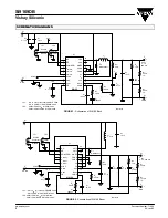
Included in this document are schematics (Figure 1 and
Figure 2), demo board sample waveform (Figure 3 through 6),
PCB layout (Figure 7 through 12), and Bill Of Material (Table 1
and 2).
The demonstration board layout is available in Gerber file format. Please contact your Vishay Siliconix sales representative or
distributor for a copy.
ORDERING INFORMATION: PART NUMBER
Si9169DBĆK (BUCK CONVERTER)
Si9169DBĆS (BOOST CONVERTER)
TEST SETUP AND OPERATION
1. Visually inspect demo board and make sure that Jumper 1
is set to Enable and Jumper 2 is set to PWM.
2. Attach an electronic load set to either resistive or current
mode to the output pins (P3 and P4) on the demo board.
Set the load current to 200 mA or equivalent resistor value.
After the converter is powered up, output load current can
be adjusted.
3. Attach a dc power supply, with at least 3-A current
capability, to the input pins (P1 and P2) on the demo board.
The input voltage can be adjusted between 2.7 and 3.6 V
for boost DB or 2.7 to 6 V for buck DB.
4. Put an oscilloscope ground on the input ground, and the
Ch1 probe on the output and connect Ch2 probe on pin 20
of Si9169 (COIL pin). The waveform for buck and boost DB
should appear approximately as shown in Figure 3 and 4,
respectively.
5. To test your DB in PSM, adjust the load to 20 mA. Then
change Jumper 2 setting to PSM. Notice the reduction of
the input current. With the same probe setup mentioned
above, the waveform for buck and boost DB should appear
approximately as shown in Figure 5 and 6, respectively.


