22
2801/2802 Power Analyzer User Guide
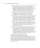
Other than the delay noted above, the turn on sequence in either AC or DC
voltage modes is the same and is timed by the Channel MCU.
Nominally 50ms after the TRIAC is turned on, the parallel relay is
engaged, and then nominally 20ms after that the TRIAC has its control
signal removed. Since the relay has a low voltage drop, there is
insufficient current flowing through the TRIAC to hold it in the on
state, and thus only the relay conducts from this point onwards.
When configured for DC voltage operation, the turn off sequence
(controlled by the channel MCU) is simply to turn off the relay
immediately after being commanded to do so by the DSP.
When configured for AC voltage operation the timing sequence during turn
off is as follows. Immediately after being commanded to turn off the
switch, the MCU turns on the control signal to the TRIAC. After
nominally 20ms the relay is turned off, and after a further nominally
40ms the TRIAC control signal is removed. In this manner the actual
load turn off is controlled by the TRIAC rather than the relay.
If the switch is used in high dV/dT situations (e.g. inductive loads), then it
may be required that the user add an external snubber circuit. This
circuitry cannot be included internally, as it is dependent on the actual
load characteristics and its presence will directly affect the off
characteristics of the switch.
Since the relay is normally the current carrying device, the TRIAC does not
limit the continuous current capability of the switch as the thermal
issues with the TRIAC are not present. The TRIAC is only used to
withstand the turn on surge of the load, and to withstand any reverse
“kick” when an AC load is turned off. Similarly, the relay is not
required to withstand the surge current of the load during turn on, nor is
it required to withstand the turn off surge of an inductive AC load, so
the requirements on the relay are reduced.
DC Offset Adjustment DACs (all inputs)
The DC Offset adjustment DACs are adjusted by the DSP (via the Channel
MCUs) to produce a zero DC reading when commanded to do so by the user.
This is accomplished independently for each input, each range, and each
current shunt selection. The DAC settings required to produce each zero DC
reading is stored independently for each combination in the Channel MCU in
non-volatile memory.
Summary of Contents for Xitron 2801
Page 1: ...USER GUIDE 2801 2802 Advanced Single and Dual Channel Power Analyzers...
Page 2: ...2 2801 2802 Power Analyzer User Guide...
Page 10: ...10 2801 2802 Power Analyzer User Guide...
Page 101: ...Printing Results 101 Figure 66 Configuration Printout...
Page 102: ...102 2801 2802 Power Analyzer User Guide Figure 67 Waveform Channel 1 Real time...
Page 103: ...Printing Results 103 Figure 68 Waveform Channe1 Distortion...
Page 104: ...104 2801 2802 Power Analyzer User Guide Figure 69 History Chart VOLTS ACDC Trends View...
Page 105: ...Printing Results 105 Figure 70 History Chart AMPS PERCENT THD Extents View...
Page 106: ...106 2801 2802 Power Analyzer User Guide Figure 71 Harmonics Listing page 1...
Page 107: ...Printing Results 107 Figure 72 Harmonics Listing page 2...
Page 145: ...Sending Commands and Interrogatives 145...
Page 147: ...Appendix A Physical Specifications 147...


