CONFIDENTIAL – DO NOT COPY
Page 8-
1
File No. SG-0184
Chapter 8 Theory of Circuit Operation
The operation of D-SUB 15pin route
The D-SUB 15pin is input analog signal to the MTK8205 transfer A/D converter then generates
the vertical and horizontal timing signals for display device.
Th
e
operation of HDMII CON route
The HDMI CON is input digital signal the signal is process to the sil9011. Then transfer to the
MTK8205, the MTK8205 generates the vertical and horizontal timing signals for display device.
The operation of HDTV & Component route
HDTV & Component signal is input to switch IDTQS3VH257 (Select Component1 or 2). Then
transfer to the MTK8205 the MTK8205 generates the vertical and horizontal timing signals for
display device.
The operation of Video 1,2,3 & S-Video route
The Video 1,2,3 and S-Video signal is transmission signal to main board MM1492 (Switch) and
output to MTK8205 the MTK8205 generates the vertical and horizontal timing signals for display
device.
The operation of TV route
TV signal is processes to the tuner and output to MM1492 (switch) then transfer to MTK8205 the
MTK8205 generates the vertical and horizontal timing signals for display device. Audio is
processes to the tuner output to SIF circuit and output to MTK8205.Then MTK8205 process to
wm8776 and output to TDA8946J transfer to speaker
The operation of DTV route
DTV signal is processes to the tuner and output to MT5111 who handle ATSC input to match MPEG-2 package,
then transfer to MT5351. After passing through decoder, the signal will be with the digital signal tri-dtate from
HDMI transfer to digital port of MT8205
The operation of keypad
There are
7
keys to control and select the function of
P42
and also has one LED to indicate the
status of operation. They are “Power,
Menu
,
CH+
,
CH-
,
VOL+
,
VOL -
, Input”.
Summary of Contents for P42HDTV10A - 42" Plasma TV
Page 1: ......
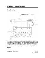
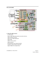
Page 27: ...CONFIDENTIAL DO NOT COPY Page 6 3 File No SG 0184 Main Board Block Diagram...
Page 60: ...CONFIDENTIAL DO NOT COPY Page 8 28 File No SG 0184...
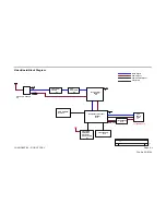
Page 61: ...CONFIDENTIAL DO NOT COPY Page 8 29 File No SG 0184 BLOCK DIAGRAM...
Page 68: ...CONFIDENTIAL DO NOT COPY Page 8 36 File No SG 0184 Fig D READ TIMING WAVEFORMS...
Page 69: ...CONFIDENTIAL DO NOT COPY Page 8 37 File No SG 0184 Fig E RESET TIMING WAVEFORM...
Page 72: ...CONFIDENTIAL DO NOT COPY Page 8 40 File No SG 0184 Pin Configuration 400mil TSOP II x4 x8 x16...
Page 94: ...CONFIDENTIAL DO NOT COPY Page 9 2 File No SG 0184 3 5V DV50A CB15 4 3 3V DV33A U5 3...
Page 95: ...CONFIDENTIAL DO NOT COPY Page 9 3 File No SG 0184 5 2 5V DV25 CE42 6 1 8V DV18A U5 2...
Page 100: ...CONFIDENTIAL DO NOT COPY Page 9 8 File No SG 0184 3 3 3V DV33 C11 4 2 5V DV25 C185...
Page 101: ...CONFIDENTIAL DO NOT COPY Page 9 9 File No SG 0184 5 1 8V DV18 C64 6 1 25V 1V25_DDR C148...
Page 102: ...CONFIDENTIAL DO NOT COPY Page 9 10 File No SG 0184 7 1 2V DV12 C26...
Page 111: ......
Page 112: ......
Page 113: ......


