CONFIDENTIAL – DO NOT COPY
Page 8-
14
File No. SG-0184
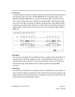
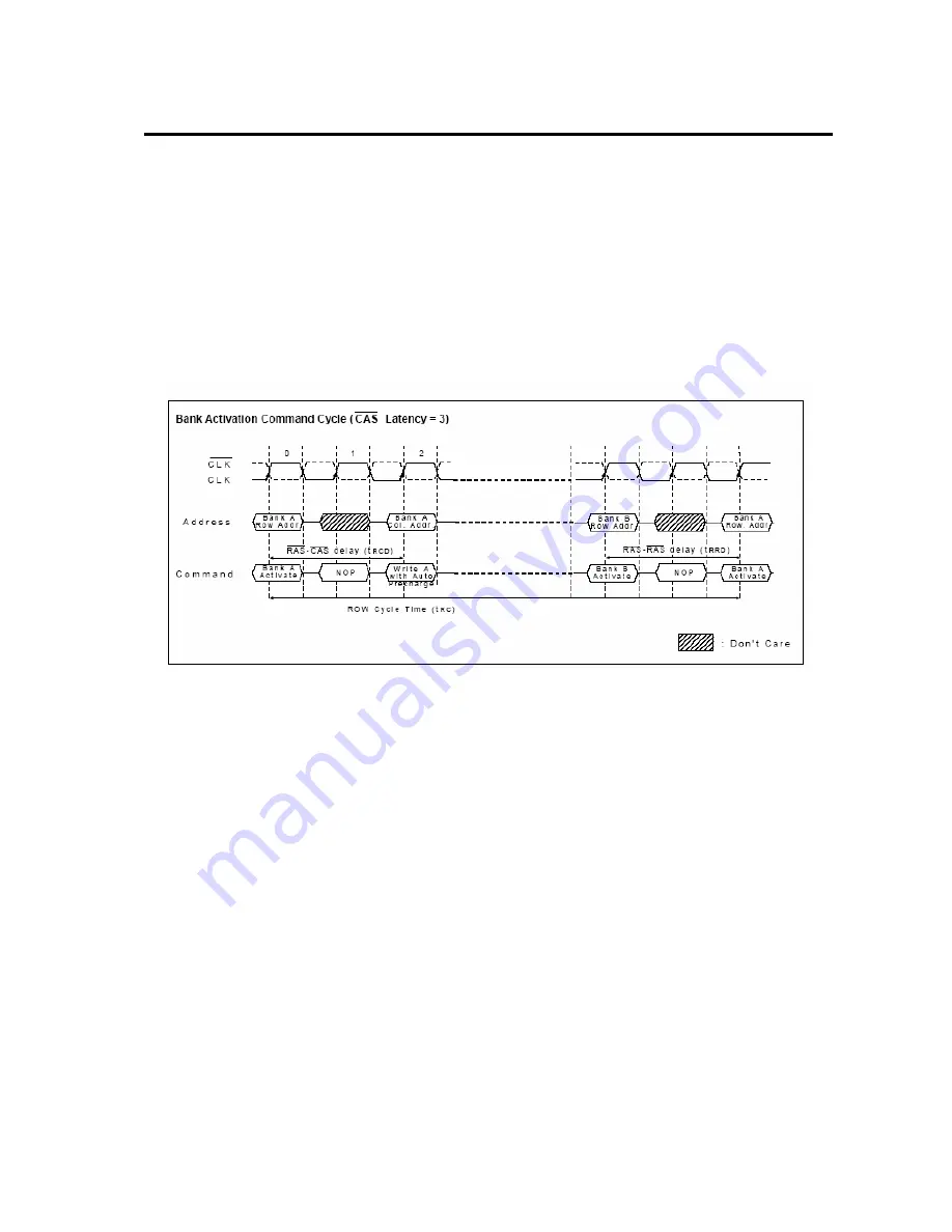
4. Row Active
The Bank Activation command is issued by holding CAS and WE high with CS and RAS low at
the rising edge of the clock (CLK). The DDR SDRAM has four independent banks; so two
Bank Select addresses (BA0, BA1) are required. The Bank Activation command to the first
read or write command must meet or exceed the minimum of RAS to CAS delay time (tRCD
min). Once a bank has been activated, it must be precharged before another Bank Activation
command can be applied to the same bank. The minimum time interval between interleaved
Bank Activation command (Bank A to Bank B and vice versa) is the Bank-to-Bank delay time
(tRRD min).
5. Read Bank
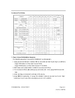
This command is used after the row activates command to initiate the burst read of data. The
read command is initiated by activating CS, CAS , and deasserting WE at the same clock
sampling (rising) edge as described in the command truth table. The length of the burst and
the CAS latency time will be determined by the values programmed during the MRS
command.
6. Write Bank
This command is used after the row activates command to initiate the burst write of data. The
write command is initiated by activating CS, CAS, and WE at the same clock sampling (rising)
edge as describe in the command truth table. The length of the burst will be determined by the
values programmed during the MRS command.
Summary of Contents for P42HDTV10A - 42" Plasma TV
Page 1: ......
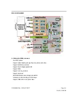
Page 27: ...CONFIDENTIAL DO NOT COPY Page 6 3 File No SG 0184 Main Board Block Diagram...
Page 60: ...CONFIDENTIAL DO NOT COPY Page 8 28 File No SG 0184...
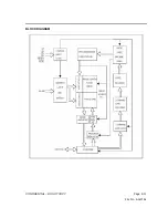
Page 61: ...CONFIDENTIAL DO NOT COPY Page 8 29 File No SG 0184 BLOCK DIAGRAM...
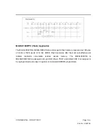
Page 68: ...CONFIDENTIAL DO NOT COPY Page 8 36 File No SG 0184 Fig D READ TIMING WAVEFORMS...
Page 69: ...CONFIDENTIAL DO NOT COPY Page 8 37 File No SG 0184 Fig E RESET TIMING WAVEFORM...
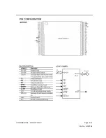
Page 72: ...CONFIDENTIAL DO NOT COPY Page 8 40 File No SG 0184 Pin Configuration 400mil TSOP II x4 x8 x16...
Page 94: ...CONFIDENTIAL DO NOT COPY Page 9 2 File No SG 0184 3 5V DV50A CB15 4 3 3V DV33A U5 3...
Page 95: ...CONFIDENTIAL DO NOT COPY Page 9 3 File No SG 0184 5 2 5V DV25 CE42 6 1 8V DV18A U5 2...
Page 100: ...CONFIDENTIAL DO NOT COPY Page 9 8 File No SG 0184 3 3 3V DV33 C11 4 2 5V DV25 C185...
Page 101: ...CONFIDENTIAL DO NOT COPY Page 9 9 File No SG 0184 5 1 8V DV18 C64 6 1 25V 1V25_DDR C148...
Page 102: ...CONFIDENTIAL DO NOT COPY Page 9 10 File No SG 0184 7 1 2V DV12 C26...
Page 111: ......
Page 112: ......
Page 113: ......


