CONFIDENTIAL – DO NOT COPY
Page 8-
34
File No. SG-0184
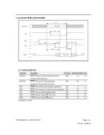
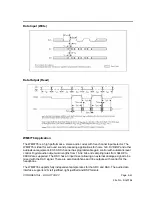
The system can thus monitor RY/BY to determine whether the reset operation is complete. If
RESET is asserted when a program or erase operation is not executing (RY/BY pin is "1"), the
reset operation is completed within a time of tREADY (not during Embedded Algorithms). The
system can read data tRH after the RESET pin returns to VIH. Refer to the AC Characteristics
tables for RESET parameters and to Figure 14 for the timing diagram.
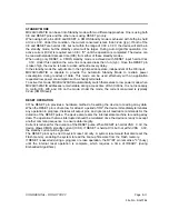
WRITE PROTECT (WP)
The write protect function provides a hardware method to protect boot sectors without using VID.
If the system asserts VIL on the WP/ACC pin, the device disables program and erase functions
in the two "outermost" 8 Kbyte boot sectors independently of whether those sectors were
protected or unprotected using the method described in Sector/Sector Group Protection and
Chip Unprotection". The two outermost 8 Kbyte boot sectors are the two sectors containing the
lowest addresses in a bottom-boot-configured device, or the two sectors containing the highest
addresses in a top-boot-configured device.
If the system asserts VIH on the WP/ACC pin, the device reverts to whether the two outermost
8K Byte boot sectors were last set to be protected or unprotected. That is, sector protection or
unprotection for these two sectors depends on whether they were last protected or unprotected
using the method described in "Sector/Sector Group Protection and Chip Unprotection".
Note that the WP/ACC pin must not be left floating or unconnected; inconsistent behavior of the
device may result.
SOFTWARE COMMAND DEFINITIONS :
Device operations are selected by writing specific address and data sequences into the
command register. Writing incorrect address and data values or writing them in the improper
sequence will reset the device to the read mode. Table 3 defines the valid register command
sequences. Note that the Erase Suspend (B0H) and Erase Resume (30H) commands are valid
only while the Sector Erase operation is in progress. Either of the two reset command sequences
will reset the device (whenapplicable).
All addresses are latched on the falling edge of WE or CE, whichever happens later. All data are
latched on rising edge of WE or CE, whichever happens first.
WRITE OPERATION STATUS
The device provides several bits to determine the status of a write operation: Q2, Q3, Q5, Q6, Q7,
and RY/BY.Table B and the following subsections describe the functions of these bits. Q7,
RY/BY, and Q6 each offer a method for determining whether a program or erase operation is
complete or in progress. These three bits are discussed first.
Summary of Contents for P42HDTV10A - 42" Plasma TV
Page 1: ......
Page 27: ...CONFIDENTIAL DO NOT COPY Page 6 3 File No SG 0184 Main Board Block Diagram...
Page 60: ...CONFIDENTIAL DO NOT COPY Page 8 28 File No SG 0184...
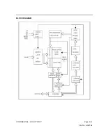
Page 61: ...CONFIDENTIAL DO NOT COPY Page 8 29 File No SG 0184 BLOCK DIAGRAM...
Page 68: ...CONFIDENTIAL DO NOT COPY Page 8 36 File No SG 0184 Fig D READ TIMING WAVEFORMS...
Page 69: ...CONFIDENTIAL DO NOT COPY Page 8 37 File No SG 0184 Fig E RESET TIMING WAVEFORM...
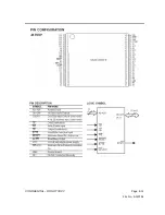
Page 72: ...CONFIDENTIAL DO NOT COPY Page 8 40 File No SG 0184 Pin Configuration 400mil TSOP II x4 x8 x16...
Page 94: ...CONFIDENTIAL DO NOT COPY Page 9 2 File No SG 0184 3 5V DV50A CB15 4 3 3V DV33A U5 3...
Page 95: ...CONFIDENTIAL DO NOT COPY Page 9 3 File No SG 0184 5 2 5V DV25 CE42 6 1 8V DV18A U5 2...
Page 100: ...CONFIDENTIAL DO NOT COPY Page 9 8 File No SG 0184 3 3 3V DV33 C11 4 2 5V DV25 C185...
Page 101: ...CONFIDENTIAL DO NOT COPY Page 9 9 File No SG 0184 5 1 8V DV18 C64 6 1 25V 1V25_DDR C148...
Page 102: ...CONFIDENTIAL DO NOT COPY Page 9 10 File No SG 0184 7 1 2V DV12 C26...
Page 111: ......
Page 112: ......
Page 113: ......

