background image

CONFIDENTIAL – DO NOT COPY


Page 8-

38


File No. SG-0184


DDR SDRAM (NT5DS16M16CS-5T) Application : 
Functional Description 

The 256Mb DDR SDRAM is a high-speed CMOS, dynamic random-access memory containing 
268, 435, 456 bits. The 256Mb DDR SDRAM is internally configured as a quad-bank DRAM. 

The 256Mb DDR SDRAM uses a double-data-rate architecture to achieve high-speed operation. 
The double-data-rate architecture is essentially a 

2n 

prefetch architecture, with an interface 

designed to transfer two data words per clock cycle at the I/O pins. A single read or write access 
for the 256Mb DDR SDRAM consists of a single 

2n

-bit wide, one clock cycle data transfer at the 

internal DRAM core and two corresponding n-bit wide, one-half clock cycle data transfers at the 
I/O pins. 

Read and write accesses to the DDR SDRAM are burst oriented; accesses start at a selected 
location and continue for a programmed number of locations in a programmed sequence. 
Accesses begin with the registration of an Active command, which is then followed by a Read or 
Write command. The address bits registered coincident with the Active command are used to 
select the bank and row to be accessed (BA0, BA1 select the bank; A0-A12 select the row). The 
address bits registered coincident with the Read or Write command are used to select the 
starting column location for the burst access. 

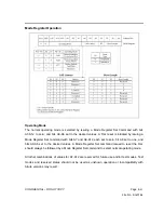
Prior to normal operation, the DDR SDRAM must be initialized. The following sections provide 
detailed information covering device initialization, register definition, command descriptions and 
device operation. 

Summary of Contents for P42HDTV10A - 42" Plasma TV

Page 1: ......

Page 2: ...Factory Preset Timings 4 1 5 Pin Assignment 5 1 6 BLOCK DIAGRAM 6 1 7 Main Board I O Connections 7 1 8 Theory of Circuit Operation 8 1 9 Waveforms 9 1 10 Trouble Shooting 10 1 11 Spare Parts List 11...

Page 3: ...o communications However there is no guarantee that the interference will not occur in a particular installation If this equipment does cause unacceptable interference to radio or television reception...

Page 4: ...M Cable NTSC Antenna Cable y All TV formats supported 480i 480p 720p 1080i y PC compatible RGB up to 1280 x 1024 WXGA y High definition digital interface HDMI y Multiple screen display picture on pict...

Page 5: ...200 cd m2 typical panel spec Min 300 cd m2 Contrast Ratio 10 000 1 Typical panel spec TV system NTSC ATSC QAM PC Inputs 15pins D sub HDMI DVI Video Inputs 1 x S Video 3 x AV inputs CVBS RCA type 2 x C...

Page 6: ...tness Min 300 cd m2 Color coordinates 9300K x 0 283 0 02 y 0 297 0 02 RGB 6500K x 0 313 0 02 y 0 329 0 02 RGB VIDEO 5000K x 0 346 0 02 y 0 359 0 02 RGB 3 Power Supply a Input voltage 100 240Vac 50 60H...

Page 7: ...DENTIAL DO NOT COPY Page 2 3 File No SG 0184 5 Dimensions Item W Stand W O stand a Height 780 mm 755 mm b Width 1072mm 1072mm c Depth 290 mm 109 mm 6 Weight a Net 38 8 0 5 kgs b Gross 47 5 1 5 kgs 0 5...

Page 8: ...Adjust the BRIGHTNESS 0 100 c Adjust the CONTRAST 0 100 d Adjust the COLOR saturation 0 100 e Adjust the TINT hue 0 100 f Adjust the SHARPNESS 0 100 g CLOSED CAPTION OFF CC1 CC2 CC3 CC4 TT1 TT2 TT3 T...

Page 9: ...OVIE RATING d ACCESS CODE EDIT E PIP SETUP a STYLE OFF PIP POP b Source AV1 AV2 AV3 ANALOG HD1 ANALOG HD2 DIGITAL HD RGB c SIZE SMALL MEDIUM LARGE d POSITION TOP LEFT TOP CENTER TOP RIGHT MIDDLE LEFT...

Page 10: ...UNE 0 100 B COLOR TEMP a COLOR TEMP User 5000K 6500K 9300K b RED 0 255 c GREEN 0 255 d BLUE 0 255 C AUDIO ADJUST a VOLUME 0 100 b BASS 50 50 c TREBLE 50 50 d BALANCE 50 50 e SURROUND ON OFF f REVERB O...

Page 11: ...0 c Adjust the CONTRAST 0 100 d Adjust the COLOR saturation 0 100 e Adjust the TINT hue 0 100 f Adjust the SHARPNESS 0 100 B AUDIO ADJUST a VOLUME 0 100 b BASS 50 50 c TREBLE 50 50 d BALANCE 50 50 e S...

Page 12: ...AV2 AV3 TV c SIZE SMALL MEDIUM LARGE d POSITION TOP LEFT TOP CENTER TOP RIGHT MIDDLE LEFT MIDDLE RIGHT BOTTOM LEFT BOTTOM CENTER BOTTOM RIGHT E SPECIAL FEATURES a LANGUAGE ENGLISH FRAN AIS ESPA OL b S...

Page 13: ...ON OFF CC1 CC2 CC3 CC4 TT1 TT2 TT3 TT4 B AUDIO ADJUST a VOLUME 0 100 b BASS 50 50 c TREBLE 50 50 d BALANCE 50 50 e SURROUND ON OFF f REVERB OFF CONCERT LIVING ROOM HALL ARENA g MUTE ON OFF h SPEAKERS...

Page 14: ...60 MIN 90 MIN 120 MIN c WIDE FORMAT NORMAL WIDE ZOOM d RESET ALL SETTING e IMAGE CLEANER DTV Mode A DTV TUNER SETUP a TIME ZONE 1 HAWALL 2 EASTTERN TIME 3 INDIANA 4 CENTRAL TIME 5 MOUNTAIN TIME 6 ARIZ...

Page 15: ...84 e CHANNEL SKIP f DIGITAL AUDIO OUT 1 PCM 2 DOLBY DIGITAL 3 OFF B CLOSED CAPTION a ANALOG CLOSED CAPTION OFF YES b DIGITAL CLOSED CAPTION OFF YES c DIGITAL CAPTION STYLE 1 AS BROADCASTER 2 CUSTOM 1...

Page 16: ...MAGENTA 3 FONT OPACITY SOLID TRANSLUCENT TRANSPARENT 4 BLACKGROUND COLOR BLACK WHITE GREEN BLUE RED CYAN YELLOW MAGENTA 5 BLACKGROUND OPACITY SOLID TRANSLUCENT TRANSPARENT 6 WINDOW COLOR BLACK WHITE...

Page 17: ...PIP table Sub MAIN AV1 AV2 AV3 COMPONENT 1 COMPONENT 2 HDMI RGB TV DTV AV1 N Y Y Y Y Y Y Y Y AV2 Y N Y Y Y Y Y Y Y AV3 Y Y N Y Y Y Y Y Y COMPONENT 1 Y Y Y N N N N Y N COMPONENT 2 Y Y Y N N N N Y N HD...

Page 18: ...59 94 N N 25 175 Windows 2 640x480 75 37 5 75 00 N N 31 500 Windows 3 720 x 400 70 31 46 70 08 N P 28 320 DOS 4 800x600 60 37 9 60 317 P P 40 000 Windows 5 800x600 75 46 9 75 P P 49 500 Windows 6 800x...

Page 19: ...Mode No Resolution 1 480i 2 480p 3 720p 4 1080i 4 HDMI DVI PC preset modes Mode No Resolution Refresh Rate Hz Horizontal Frequency KHz Vertical Frequency Hz Horizontal Sync Polarity TTL Vertical Sync...

Page 20: ...ance 75 e Synchronization H V separate sync H V composite sync Sync on Green TTL TTL f Video bandwidth 135MHz g Connector type 15 pin D Sub female 5 11 1 6 10 15 5 10 15 1 6 11 Pin Number Pin Assignme...

Page 21: ...pe A d Pin Assignment Please see below Pin Signal Assignment Pin Signal Assignment 1 TMDS Data2 2 TMDS Data2 Shield 3 TMDS Data2 4 TMDS Data1 5 TMDS Data1 Shield 6 TMDS Data1 7 TMDS Data0 8 TMDS Data0...

Page 22: ...S Video Connector a Frequency H 15 734KHz V 60Hz NTSC b Signal level Y 1Vp p C 0 286Vp p c Impedance 75 d Connector type 4 pin mini DIN 5 Component video Connector a Frequency H 15 734KHz V 60Hz NTSC...

Page 23: ...z QAM system supporting clear QAM a IF output level 1Vp p minimum b Frequency 57 849 MHz 7 PC Stereo audio a Signal level 1Vrms b Impedance 47K c Connector type 3 5 mini jack 8 Video Stereo audio a Si...

Page 24: ...nce 47K c Frequency Response 250Hz 20KHz d Connector type RCA L R 2 Digital audio out a Peak emission wave length 630 690 m b Transmission Speed 13 2M pbs c Connector type Optical fiber transmitter 3...

Page 25: ...AC source of 100V 240V AC 10 50 60 HZ into system request power source The main board receives different types of video signal into the MTK8205 Ic Afterward the MTK8205 Ic process the signals control...

Page 26: ...volume bass treble surround and balance The HDMI video and audio is must transmitting to sil9011 processed then TMDS signal to the MTK8205 generates the vertical and horizontal timing signals for dis...

Page 27: ...CONFIDENTIAL DO NOT COPY Page 6 3 File No SG 0184 Main Board Block Diagram...

Page 28: ...S3VH257 Doc RevCode Title B 1 1 Monday November 14 2005 Title Size Document Number Rev Date Sheet of DTV Backend Decoder MT5351 U10 For Main Board Demodulator MT5111 U9 FCC 50PIN CON J1 VOLTAGE CONTRO...

Page 29: ...I o Connections J7 CONNECTION TOP BOTTOM Pin Description 1 Auto 2 Left 3 Right 4 Down 5 Gnd 6 Up 7 Menu 8 Source 9 Power 10 LED 11 IR 12 5V J1 CONNECTION TOP BOTTOM Pin Description 1 POWRSW 2 12V 3 1...

Page 30: ...OT COPY Page 7 2 File No SG 0184 J3 CONNECTION TOP BOTTOM Pin Description 1 SVDET2 2 S1C_GND 3 S1C_IN 4 S1Y_GND 5 S1Y_IN 6 AGND 7 AV3R 8 AV3R GND 9 AV3L 10 AV3_GND 11 AV3_IN 12 AV3L GND 13 HPL 14 HPDE...

Page 31: ...READY 29 VOG1 5 ORESET 30 VOG0 6 GND 31 GND 7 VOPCLK 32 VOB7 8 VODE 33 VOB6 9 VOVSYNC 34 VOB5 10 VOHSYNC 35 VOB4 11 GND 36 GND 12 VOR7 37 VOB3 13 VOR6 38 VOB2 14 VOR5 39 VOB1 15 VOR4 40 VOB0 16 GND 41...

Page 32: ...CONFIDENTIAL DO NOT COPY Page 7 4 File No SG 0184 J8 CONNECTION TOP BOTTOM Pin Description 1 5V 2 GND 3 GND 4 12V 5 12V...

Page 33: ...d S Video signal is transmission signal to main board MM1492 Switch and output to MTK8205 the MTK8205 generates the vertical and horizontal timing signals for display device The operation of TV route...

Page 34: ...to HDTV It includes 3D comb filter TV Decoder to retrieve the best image from popular composite signals On chip advanced motion adaptive de interlacer converts accordingly the interlace video into pr...

Page 35: ...CONFIDENTIAL DO NOT COPY Page 8 3 File No SG 0184 BOLOCK DIAGRAM 1 Video input a Input Multiplexing 1 component X2 2 composite X3 3 s videoX1 4 HDMI X1 5 VGA X1 6 RF X2...

Page 36: ...em Frequency 55 801MHZ 7 support ATSC system Frequency 57 863MHZ 2 TV Decoder For pip pop Dual identical TVD on chip 3D comb for both path Dual VBI decoders for the application of V chip 3 Support For...

Page 37: ...nes Support alpha blending among these two planes and video Support text bitmap decoder Support line rectangle gradient fill Support bitblt Support color key function Support clip mask 65535 256 16 4...

Page 38: ...nput Output AE26 VGASDA Input Output AB23 REQUEST Input Output AB24 READY Input Output AD22 SCL Input Output AC22 SDA Input Output OBO0 SOURCE Input Key detection OBO1 MENU Input Key detection OBO2 UP...

Page 39: ...ital HD1 HDMI H X 9 9 9 9 X X X X RGB I X 9 9 9 9 X X X X Input Matrix for Windowing Functionality 6 Video processor a Color management Flesh tone and multiple color enhancement Gamma anti Gamma corre...

Page 40: ...a scaling Programmable Zoom viewer Picture in picture PIP Picture in picture d Display 12 10 10 8 8 6 Dithering processing for PDP display 10bit gamma correction Support Alpha blending for Video and t...

Page 41: ...T COPY Page 8 9 File No SG 0184 8 Flash Usage Flash is used to store FW code fonts bitmaps and big tables for VGA Video and Gamma 2Mbyte is recommended to build a general TV model MTK8205 Flash ROM su...

Page 42: ...CONFIDENTIAL DO NOT COPY Page 8 10 File No SG 0184 DDR SDRAM M13S128168A 6T Application Pin description...

Page 43: ...be undefined Apply VDD before or at the same time as VDDQ Apply VDDQ before or at the same time as VTT VREF 2 Start clock and maintain stable condition for a minimum of 200us 3 The minimum of 200us a...

Page 44: ...t be written after EMRS setting for proper DDR SDRAM operation The mode register is written by asserting low on CS RAS CAS WE and BA0 The DDR SDRAM should be in all bank recharge with CKE already high...

Page 45: ...rge each bank respectively or all banks simultaneously The bank select addresses BA0 BA1 are used to define which bank is precharged when the command is initiated For write cycle tWR min must be satis...

Page 46: ...ivation command Bank A to Bank B and vice versa is the Bank to Bank delay time tRRD min 5 Read Bank This command is used after the row activates command to initiate the burst read of data The read com...

Page 47: ...and rising edge of Data Strobe DQS adopted by DDR SDRAM until the burst length is completed 8 Burst Write Operation The Burst Write command is issued by having CS CAS and WE low while holding RAS high...

Page 48: ...y organized as 1M bytes of 8 bits or 512K words of 16 bits MXIC s Flash memories offer the most cost effective and reliable read write non volatile random access memory The MX29LV800T B MX29LV800AT AB...

Page 49: ...and data sequences into the command register Writing incorrect address and data values or writing them in the improper sequence will reset the device to the read mode Table 5 defines the valid regist...

Page 50: ...e using both standard and Unlock Bypass command sequences An erase operation can erase one sector multiple sectors or the entire device Table indicates the address space that each sector occupies A se...

Page 51: ...tics table represents the active current specification for the write mode The AC Characteristics section contains timing specification table and timing diagrams for write operations Figure 1 3 READ RE...

Page 52: ...ection next 5 RESET COMMAND Writing the reset command to the device resets the device to reading array data Addresses bits are don t care for this command The reset command may be written between the...

Page 53: ...ce MT5111 accepts either the direct IF signals centered at 44MHZ or 43 75MHZ or the low IF signal Centered at 5 38MHZ The center frequency of the incoming IF signal can also be programmed to other fre...

Page 54: ...ransport stream packets The chip finally outputs the decoded MPEG 2 packets in either the serial or parallel transport stream format In addition to the demodulation of HDTV signal MT5111 also provides...

Page 55: ...pport flexible transport demux HD MPEG 2 video decoder JPEG decoder MPEG1 2 MP3 AC3 audio decoder HDTV encoder The MT5351 enables consumer electronics manufactures to build high quality feature rich D...

Page 56: ...pport TS recording via IEEE1394 interface C MPEG2 Decoder 1 Support dual MPEG 2 HD decoder or up to 8 SD decoder 2 Complaint to MP ML MP HL and MPEG 1 video standards D JPEG Decoder 1 Decode Base line...

Page 57: ...icture PIP 5 Picture Out Picture POP 6 480i 576i 480p 576p 720p 1080i output I Auxiliary Display 1 Mixing one video and one OSD 2 480i 576i output J TV Encoder 1 Support NTSC M N PAL M N B D G H I 2 M...

Page 58: ...round processing include virtual surround 10 Audio and video lip synchronization 11 Support reverberation 12 SPDIF out 13 I2S I F O Peripherals 1 Three UARTs with Tx and Rx FIFO two of them have hardw...

Page 59: ...nd output enable OE controls MXIC s Flash memories augment EPROM functionality with in circuit electrical erasure and programming The MX29LV320AT B uses a command register to manage this functionality...

Page 60: ...CONFIDENTIAL DO NOT COPY Page 8 28 File No SG 0184...

Page 61: ...CONFIDENTIAL DO NOT COPY Page 8 29 File No SG 0184 BLOCK DIAGRAM...

Page 62: ...ions may also be implemented via programming equipment See the Sector Group Protection and Chip Unprotection section 3 If WP ACC VIL the two outermost boot sectors remain protected If WP ACC VIH the t...

Page 63: ...er command sequences Writing incorrect address and data values or writing them in the improper sequence resets the device to reading array data Section has details on erasing a sector or the entire ch...

Page 64: ...eset command is required to return to the read mode when the device is in the Automatic Select mode or if Q5 goes high 4 The fourth cycle of the Automatic Select command sequence is a read cycle 5 The...

Page 65: ...low power consumption such as handy terminals To active this mode MX29LV320AT B automatically switch themselves to low power mode when MX29LV320AT B addresses remain stable during access time of tACC...

Page 66: ...sectors were last set to be protected or unprotected That is sector protection or unprotection for these two sectors depends on whether they were last protected or unprotected using the method describ...

Page 67: ...ed sector will cause Q2 to toggle 2 Performing successive read operations from any address will cause Q6 to toggle 3 Reading the byte word address being programmed while in the erase suspend program m...

Page 68: ...CONFIDENTIAL DO NOT COPY Page 8 36 File No SG 0184 Fig D READ TIMING WAVEFORMS...

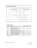
Page 69: ...CONFIDENTIAL DO NOT COPY Page 8 37 File No SG 0184 Fig E RESET TIMING WAVEFORM...

Page 70: ...and two corresponding n bit wide one half clock cycle data transfers at the I O pins Read and write accesses to the DDR SDRAM are burst oriented accesses start at a selected location and continue for...

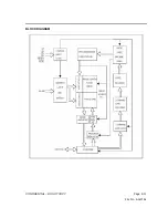
Page 71: ...Functional Block Diagram is intended to facilitate user understanding of the operation of the device it does not represent an actual circuit implementation Note DM is a unidirectional signal input onl...

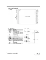
Page 72: ...CONFIDENTIAL DO NOT COPY Page 8 40 File No SG 0184 Pin Configuration 400mil TSOP II x4 x8 x16...

Page 73: ...Register Set command with bits A7 and A9 A12 each set to zero bit A8 set to one and bits A0 A6 set to the desired values A Mode Register Set command issued to reset the DLL should always be followed...

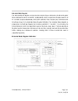
Page 74: ...are controlled via the bit settings shown in the Extended Mode Register Definition The Extended Mode Register is programmed via the Mode Register Set command with BA0 1 and BA1 0 and retains the store...

Page 75: ...h Auto Precharge disabled this command is undefined and should not be used for read bursts with Auto Precharge enabled or for write bursts 9 Deselect and NOP are functionally interchangeable Active Th...

Page 76: ...persistent so it must be issued each time a refresh is required The refresh addressing is generated by the internal refresh controller This makes the address bits Don t Care during an Auto Refresh com...

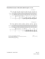
Page 77: ...along with output data The initial low state on DQS is known as the read preamble the low state coincident with the last data out element is known as the read postamble Upon completion of a burst ass...

Page 78: ...CONFIDENTIAL DO NOT COPY Page 8 46 File No SG 0184 Random Read Accesses CAS Latencies Burst Length 2 4 or 8...

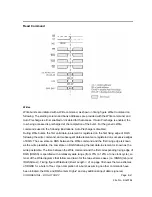
Page 79: ...owing the write command and subsequent data elements are registered on successive edges of DQS The Low state on DQS between the Write command and the first rising edge is known as the write preamble t...

Page 80: ...on any positive edge of clock following the previous Write command The first data element from the new burst is applied after either the last element of a completed burst or the last desired data ele...

Page 81: ...Etch ADC channel has programmable gain control with automatic level control Digital audio output word lengths from 16 32 bits and sampling rates from 32kHZ to 96KHZ are supported The DAC has an input...

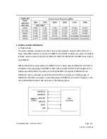
Page 82: ...ate The master clock is used to operate the digital filters and the noise shaping circuits In slave mode the WM8776 has a master detection circuit that automatically determines the relationship betwee...

Page 83: ...RC ADCBCLK DACBCLK are input to the WM8776 DIN and DACLRC are sampled by the WM8776 on the rising edge of DACBCLK ADCLRC is sampled on the rising edge of ADCBCLK ADC data is output on DOUT and changes...

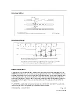
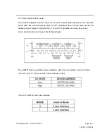
Page 84: ...d each device has a uni ue 7 bit address this is not the same as the 7 bit address of each register in the wm8776 The wm8776 operates as a slave device only 2 wire serial interface as shown in the fol...

Page 85: ...mplete solution for receiving HDMI compliant digital audio and video Specialized audio and video processing is available within the sil9011 to easily and cost effectively adds HDMI capability to consu...

Page 86: ...can monitor the presence of this 5V supply and if and when necessary provide a fast audio mute without pops when it senses the HDMI cable pulled The microcontroller can also poll registers in the sil9...

Page 87: ...ing up to 400KHZ This bus is used to configure the SIL9011 by reading writing to the appropriate registers The SIL9011 is accessible on the local I2 c bits at two device address The logic state of the...

Page 88: ...ta are transmitted and received in the units of byte and Acknowledge It is transmitted by MSB first from the Start conditions The data format is set as shown in the following figure In the L32 TV MM14...

Page 89: ...CONFIDENTIAL DO NOT COPY Page 8 57 File No SG 0184 2 Switch control table a Video output 1 b Audio output 1 c Audio gain...

Page 90: ...guration The TDA8946AJ inputs can be driven symmetrical floating as well as asymmetrical In the asymmetrical mode one input pin is connected via a capacitor to the signal source and the other input is...

Page 91: ...8 59 File No SG 0184 2 Output power measurement The output power as a function of the supply voltage is measured on the output pins at THD 10 in the L32 LCD TV Vcc 12V so we can see as shown in the fo...

Page 92: ...the proper DC voltage to pin MODE a Mute In this mode the amplifier is DC biased but not operational no audio output This allows the input coupling capacitors to be charged to avoid pop noise The dev...

Page 93: ...CONFIDENTIAL DO NOT COPY Page 9 1 File No SG 0184 Chapter 9 Waveforms Main Board 1 Voltage Measurement 1 12V DV120B U6 1 2 9V AV_V90 U6 3...

Page 94: ...CONFIDENTIAL DO NOT COPY Page 9 2 File No SG 0184 3 5V DV50A CB15 4 3 3V DV33A U5 3...

Page 95: ...CONFIDENTIAL DO NOT COPY Page 9 3 File No SG 0184 5 2 5V DV25 CE42 6 1 8V DV18A U5 2...

Page 96: ...CONFIDENTIAL DO NOT COPY Page 9 4 File No SG 0184 2 Clock Timing 1 MT8205 Clock Ch1 U9 A15 XTALI Ch2 U9 B15 XTALO 2 Memory Clock Ch1 U11 45 D_CLK Ch2 U12 45 D_CLK...

Page 97: ...CONFIDENTIAL DO NOT COPY Page 9 5 File No SG 0184 3 Sil 9011 Clock Ch1 U16 85 XTLI Ch2 U16 84 XTLO...

Page 98: ...CONFIDENTIAL DO NOT COPY Page 9 6 File No SG 0184 3 H sync V sync Timing 1 PC Mode 1024 x 768 60Hz Ch1 H sync FB46 Ch2 V sync FB45...

Page 99: ...CONFIDENTIAL DO NOT COPY Page 9 7 File No SG 0184 ATSC Board 1 Voltage Measurement 1 12V 12V C4 2 5V 5V C239...

Page 100: ...CONFIDENTIAL DO NOT COPY Page 9 8 File No SG 0184 3 3 3V DV33 C11 4 2 5V DV25 C185...

Page 101: ...CONFIDENTIAL DO NOT COPY Page 9 9 File No SG 0184 5 1 8V DV18 C64 6 1 25V 1V25_DDR C148...

Page 102: ...CONFIDENTIAL DO NOT COPY Page 9 10 File No SG 0184 7 1 2V DV12 C26...

Page 103: ...CONFIDENTIAL DO NOT COPY Page 9 11 File No SG 0184 2 Clock Timing 1 MT5351 Clock Timing U10 B2 OXTALI 2 MT5111 Clock Timing U9 97 XTAL1 96 XTAL2 Ch1 XTAL1 Ch2 XTAL2...

Page 104: ...CONFIDENTIAL DO NOT COPY Page 9 12 File No SG 0184 3 Memory Clock Timing U13 45 MEM_CLKA 4 Memory Clock Timing U12 45 MEM_CLKA...

Page 105: ...nector good 3 Is DC DC OK 4 Is U4 3 3V working ok LED is lighting It is in power saving 1 Check video cable 2 Is the timing supported 3 Check sync input 4 Check VGASOG rout if analog SOG It means data...

Page 106: ...Input signal 1 Check video 2 Check DVD player U20 input 1 Check P2 signal 2 Check signal between P2 and U20 IF AV1 AV2 mode 3 Check Tuner U20 IF TV mode LVDS output 1 Check signal between U20 and U9...

Page 107: ...COMPONENT1 2 IS NOT DISPLAY CORRECTLY Start Input signal 1 Check video 2 Check host s setting U21 input 1 Check signal between P8 U21 U9 input 1 Check signal between U21 U9 2 Check U9 Clock 27MHZ LVD...

Page 108: ...Ye HDMI IS NOT DISPLAY CORRECTLY Input signal Start 1 Check video 2 Check host s setting U16 input 1 Check p1 connect 2 Check signal between P1 and U16 U16 no data 1 Check U16 power 2 Check between s...

Page 109: ...k power cable connection J1 U7 pin 5 6 7 8 The voltage is about 5V while power switch on 1 J1 connection good 2 Check U9 GPIO Pin U4 pin2 The voltage is about 3 3V 1 J1 to connection good 2 Check U4 U...

Page 110: ...N0 TROUBLE OF DDC READING Start Analog DDC Support DDC1 2B 1 Analog cable ok 2 Check signal U18 to P3 3 Check U18 Voltage 4 Is compliant protocol HDMIDDC Support DDC1 2B 1 Analog cable ok 2 Check sign...

Page 111: ......

Page 112: ......

Page 113: ......

Reviews: