13 CUSTOMIZED ISOLATION OF P2A/C
The input channels on the VBT-325 are designed for 'ITL/CMOS voltage
levels only (0.0-5.0V), and damage may occur if other voltages are applied.
If the P2
bus contains signals with voltage levels other than ITL/CMOS, (for
example ECL, analogue or special power supply voltages as found in VXI
systems), these must be isolated from the VBT-325.
(For analysis of VX1 systems, VMETRO is developing an adapter that will
include the necessary isolation and even ECL to Tl'L conversion, part # VXA-
035. Available 1Q94.)
If the P2 pins cannot be isolated by means of selecting another slot or by using
an isolating extender board, your VBT-325 board can be customized by cutting
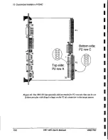
copper tracks that are specially laid out for all P2 signals for this purpose.
These can be found as a row of 32 pairs or solder pads connected with a thin
copper track on each side of the board just next to the P2 connector. The pads
on the bottom side are signals from P2 row C, and the top side row A. Please
refer to figure A7 on the next page for details.
NB: Cut very carefully with a thin, sharp surgeon knife, and cut the
surface only to avoid damaging inner layers.
If
a connection needs to be re-established, a short piece of un-isolated wire
(AWG30 or similar) can be soldered between the two pads in a pair.
NB: Before performing any cuts, please contact
VMETRO for approval regarding warranty.
VMETRO
V
B
T
-
3
2
5
User's Manual
1
4
9
Summary of Contents for VBAT-PB
Page 15: ...x i v 1 1 I 1 1 I I i i I I 1 I I 1 I 1 I I ...
Page 23: ...1VBT 325 Product overview 8 V B T 3 2 5 User s Manual V M E T R O ...
Page 125: ...8 Trace examples 110 V B T 3 2 5 User s Manual V M E T R O ...
Page 144: ...9 VBAT PB VME bus anomaly trigger ITP40 I GND VMETRO V B T 3 2 5 User s Manual 1 2 9 ...
Page 159: ...1 1Jumper settings 144 V B T 3 2 5 User s Manual V M E T R O ...
Page 181: ...16 Simulator for PC 166 V B T 3 2 5 User s Manual V M E T R O ...


