background image

500-003124-000

5-5

5.4

ANALOG INPUT CONNECTOR DESCRIPTION

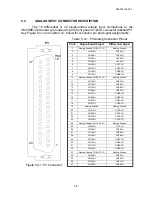
The 16 differential or 32 single-ended analog input connections to the 

VMIVME-3124 board are made using the front panel 37-pin D connector labelled P3. 
See Figure 5.4-1 and Table 5.4-1 below for connector pin and signal assignments.

Table  5.4-1. P3 Analog Connector Pinout 

Pin #

Single-Ended Signal

Differential Signal

1

Analog Ground CH 24-31 LO

Analog Ground

2

CH30-HI

CH15-HI

3

CH28-HI

CH14-HI

4

CH26-HI

CH13-HI

5

CH24-HI

CH12-HI

6

CH23-HI

CH11-LO

7

CH21-HI

CH10-LO

8

CH19-HI

CH09-LO

9

CH17-HI

CH08-LO

10

Analog Ground CH 08-15 LO

Analog Ground

11

CH14-HI

CH07-HI

12

CH12-HI

CH06-HI

13

CH10-HI

CH05-HI

14

CH08-HI

CH04-HI

15

CH07-HI

CH03-LO

16

CH05-HI

CH02-LO

17

CH03-HI

CH01-LO

18

CH01-HI

CH00-LO

19

Analog Ground

Analog Ground

20

CH31-HI

CH15-LO

21

CH29-HI

CH14-LO

22

CH27-HI

CH13-LO

23

CH25-HI

CH12-LO

24

Analog Ground CH 16-23 LO

Analog Ground

25

CH22-HI

CH11-HI

26

CH20-HI

CH10-HI

27

CH18-HI

CH09-HI

28

CH16-HI

CH08-HI

29

CH15-HI

CH07-LO

30

CH13-HI

CH06-LO

31

CH11-HI

CH05-LO

32

CH09-HI

CH04-LO

33

Analog Ground CH 00-07 LO

Analog Ground

34

CH06-HI

CH03-HI

35

CH04-HI

CH02-HI

36

CH02-HI

CH01-HI

37

CH00-HI

CH00-HI

Figure 5.4-1. P3 Connector

Pin#

19

P3

37

20

1

Summary of Contents for VMIVME-3124

Page 1: ...uy your excess underutilized and idle equipment along with credit for buybacks and trade ins Custom engineering so your equipment works exactly as you specify Critical and expedited services Leasing R...

Page 2: ...UT BOARD PRODUCT MANUAL DOCUMENT NO 500 003124 000 B Revised June 10 1996 VME MICROSYSTEMS INTERNATIONAL CORPORATION 12090 SOUTH MEMORIAL PARKWAY HUNTSVILLE ALABAMA 35803 3308 205 880 0444 800 322 361...

Page 3: ...tandard Conditions of Sale AMXbus BITMODULE COSMODULE DMAbus IOWorks IOWorks Access IOWorks Foundation MAGICWARE MEGAMODULE PLC ACCELERATOR QUICK R NET Soft Logic Link SRTbus TESTCAL The Next Generati...

Page 4: ...F REVISIONS REVISION LETTER DATE PAGES INVOLVED CHANGE NUMBER VME MICROSYSTEMS INT L CORP 12090 South Memorial Parkway Huntsville AL 35803 3308 205 880 0444 REV LTR PAGE NO ii Release Cover Pages ii i...

Page 5: ...es a definite safety hazard KEEP AWAY FROM LIVE CIRCUITS Operating personnel must not remove product covers Component replacement and internal adjustments must be made by qualified maintenance personn...

Page 6: ...fault Before operating the equipment terminal marked with this symbol must be connected to ground in the manner described in the installation operation manual Frame or chassis terminal A connection to...

Page 7: ...ND DUAL PORTED RAM MEMORY 3 5 3 9 BOARD ID REGISTER 3 6 3 10 BUILT IN POWER CONVERTER AND ADC POWER SUPPLY 3 6 SECTION 4 PROGRAMMING 4 1 MEMORY MAP 4 1 4 2 REGISTER DESCRIPTIONS 4 4 4 2 1 Board ID Reg...

Page 8: ...2 5 3 1 VMIVME 3124 Configuration Jumper Locations 5 2 5 4 1 P3 Connector 5 5 LIST OF TABLES Table Page 4 1 1 VMIVME 3124 Memory Map Differential Inputs Normal Buffer 4 1 4 1 2 VMIVME 3124 Memory Map...

Page 9: ...ss and the access mode are fully selectable In short I O space the board can be ordered to support optional current inputs 0 25 mA using 32 channel single ended inputs Some of the distinguishing featu...

Page 10: ...gn extension This data is stored in on board dual ported memory for easy access The Built In Test BIT capability permits the user to verify the on board ADC using high precision user programmable refe...

Page 11: ...500 003124 000 2 1 SECTION 2 PHYSICAL DESCRIPTION AND SPECIFICATIONS REFER TO 800 003124 000 SPECIFICATION...

Page 12: ...be digitized every 25 sec The following sections discuss the functional components of the VMIVME 3124 in detail 3 2 FUNCTIONAL ORGANIZATION The VMIVME 3124 is divided into the following functional cat...

Page 13: ...ol signals are ignored unless the board selection comparator detects a match between the on board selection jumpers and the address and address modifier line from the backplane The appropriate board r...

Page 14: ...channel In either case the electrical process of analog to digital conversion is similar The VMIVME 3124 uses a 12 bit ADC The ADC has a conversion time of 8 5 sec Settling time is required for the m...

Page 15: ...scans all 16 or 32 channels in a normal mode of operation If the mode bit is set in the CSR channel 0 will correspond to the selected reference voltage VREF0 VREF1 VREF2 or Analog Ground according to...

Page 16: ...the single ended or differential mode of operation The second tier multiplexer also selects the BIT reference voltage if enabled in the Control Status Register The second tier output is differentiall...

Page 17: ...lows the controlling software to lock onto a channel and digitize it at the maximum rate of 40 kHz Please note that the desired channel can not be directly set The software must wait for the desired c...

Page 18: ...4 1 2 applies If the board is jumpered for single ended inputs Table 4 1 3 is the only map that applies see Section 5 for details concerning setting the input configuration jumpers Table 4 1 1 VMIVME...

Page 19: ...9 Data word read write 54 Channel 10 Data word read write 56 Channel 11 Data word read write 58 Channel 12 Data word read write 5A Channel 13 Data word read write 5C Channel 14 Data word read write 5E...

Page 20: ...read write 54 Channel 10 Data word read write 56 Channel 11 Data word read write 58 Channel 12 Data word read write 5A Channel 13 Data word read write 5C Channel 14 Data word read write 5E Channel 15...

Page 21: ...It contains two bits of configuration status information each determined by the state of jumpers on the board See Table 4 2 2 1 for the definition of these bits The Input Mode bit indicating single en...

Page 22: ...e Data Register pointed to by the Channel Pointer Register is updated although it will be updated much faster than usual approximately every 25 sec The best way to stop on a single desired channel is...

Page 23: ...data pages get updated and each input is converted in two separate passes The Channel Pointer Register can be used to determine which of the two Data Registers has been most recently updated The addr...

Page 24: ...om Table 4 2 5 1 Two other values necessary to determine the meaning of the values in the Data Registers the Channel Pointer Register and the Max Buffer bit both previously described The Channel Point...

Page 25: ...r Register must be read to determine which of the two data sets is most recent In this case the Channel Pointer Register value does not hold a channel number but an offset value into the extended data...

Page 26: ...oltage stimulus and attempt to determine the current gain and range settings by comparing the data to the values in Tables 4 3 1 through 4 3 3 This technique is not recommended however since the board...

Page 27: ...r while the data is being updated preferably one should access a channel immediately after it has been updated Interrupts should always be disabled before accessing a Data Register to avoid the possib...

Page 28: ...erved All items should be carefully unpacked and thoroughly inspected for damage that might have occurred during shipment The board s should be checked for broken components damaged printed circuit bo...

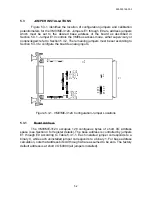
Page 29: ...board s analog inputs P1 E1 E3 E4 E5 E6 E2 E8 E9 E7 E 1 0 E1 6 E1 3 E12 E11 E1 4 E 1 5 E17 E18 E 19 E20 R56 R53 R54 R65 R64 R60 TP2 TP1 Figure 5 3 1 VMIVME 3124 Configuration Jumper Locations 5 3 1 B...

Page 30: ...g from the least significant bit Then check Table 5 3 1 1 All clear bits should have a jumper installed on the corresponding address bit jumper and all set bits should have a jumper removed For exampl...

Page 31: ...E14 E15 install E16 RANGE 10 V range Install jumpers E19 pins 1 2 E20 pins 2 3 5 V range Install jumpers E19 pins 1 2 E20 pins 1 2 0 10 V range Install jumpers E19 pins 2 3 E20 pins 1 2 GAIN unity gai...

Page 32: ...1 HI CH10 LO 8 CH19 HI CH09 LO 9 CH17 HI CH08 LO 10 Analog Ground CH 08 15 LO Analog Ground 11 CH14 HI CH07 HI 12 CH12 HI CH06 HI 13 CH10 HI CH05 HI 14 CH08 HI CH04 HI 15 CH07 HI CH03 LO 16 CH05 HI CH...

Page 33: ...ocedure center potentiometer R53 c Attach DVM positive to ADC input at TP1 attach negative to analog ground at TP2 d Short the channel 0 input HI and LO inputs e Halt scanning on channel 0 f Adjust in...

Page 34: ...nning on channel 0 and monitor channel 0 data e Adjust bipolar offset potentiometer R64 until channel 0 data fluctuates between 000 and 001 f Adjust precision voltage source to 4 996338 VDC g Adjust g...

Page 35: ...only after the instrumentation amp and appropriate offset and gain calibration procedures a Attach DVM positive to ADC input at TP1 attach negative to analog ground at TP2 b Halt scanning on channel...

Page 36: ...their proper connector location f Connector pins are clean and free from contamination g No components of adjacent boards are disturbed when inserting or removing the board from the chassis h Quality...

Page 37: ...s IOWorks Foundation Visual Soft Logic Control ler MAGICWARE VMEaccess MEGAMODULE VMEmanager PLC ACCELERATOR VMEmonitor QUICK R NET VMEnet Soft Logic Link VMEnet II SRTbus VMEprobe TESTCAL WinUIOC The...

Page 38: ...APPENDIX A ASSEMBLY DRAWING PARTS LIST AND SCHEMATIC...

Page 39: ...uipment Have surplus equipment taking up shelf space We ll give it a new home Learn more Visit us at artisantg com for more info on price quotes drivers technical specifications manuals and documentat...

Reviews: