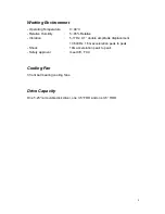
The +3.3V and +5V total output shall not exceed 100watts, and the total output for
this subject power supply is 170 watts. Ripple and noise measurements shall be
made under all specified load conditions through a single pole low pass filter with
20MHz cutoff frequency. Outputs shall bypassed at the connector with a 0.1uF
ceramic disk capacitor and a 10uF electrolytic capacitor to simulate system loading.
LOAD CAPACITY SPECIFICATIONS
The cross regulation defined as follows, the voltage regulation limits DC include DC
Output ripple & noise.
LOAD
STM.
+3.3V
+5V
+12V
-5V
-12V
ALL MAX
HHHHH
12.0A
14.0A
4.0A
0.3A
0.8A
+5V MAX
other MIN
LHLLL
0.3A
16.0 A
0.1A
0A
0A
+3.3V MAX
other MIN
HLLLL
12.0 A
1.5 A
0.1A
0A
0A
+12V MAX
other MIN
LLHLL
0.3A
3.0 A
5.0A
0A
0A
ALL MIN
LLLLL
0.3 A
1.5 A
0.1A
0A
0A
HOLD-UP TIME (@FULL LOAD)
115V / 60Hz : 17 mSec. Minimum.
230V / 50Hz : 17 mSec. Minimum.
OUTPUT RISE TIME
(10% TO 90% OF FINAL OUTPUT VALUE, @FULL LOAD)
115V-rms or 230V-rms + 5Vdc : 20ms Maximum
OVER VOLTAGE PROTECTION
+5Vdc output: +5.58Vdc minimum, + 6.82Vdc maximum
+ 3.3Vdc output: +3.5Vdc minimum, + 4.5Vdc maximum
SHORT CIRCUIT PROTECTION
Output short circuit is defined to be a short circuit load of less than 0.1 ohm.
POWER GOOD SIGNAL
TTL signal asserted (low state) : less than 0.5V while sinking 10mA.
TTL signal asserted (high state): greater than 4.75V while sourcing 500uA.
High state output impedance: less or equal to 1Kohm from output to common.
POWER GOOD @ 115/230V,FULL LOAD
100 –500mSec.
POWER FAIL @115/230V, FULL LOAD
1 mSec. minimum

