(multiplier 1 K) by switching 500
resistors in parallel
with the 5
basic current setting resistors R326,
R38, R48 and R330 producing the output frequencies
for these ranges. The four ranges below multiplier set-
ting 100 all have the same integrating current and tim-
ing capacitor as the 100 multiplier range, but for each
of these ranges, 90%, 99%, 99.9% and 99.99% of
the integrating current is subtracted by the
capacitance multiplier circuit.
4.2.4
Capacitance
Multiplier
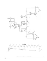
For the frequency ranges associated with multiplier
positions of 10 through 0.01, a capacitance multiplier
circuit (main board schematic, sheet I), senses the
timing capacitor charging current and subtracts the
appropriate amount so that the effective charging cur-
rent is a fraction of that delivered by the current
sources. This is accomplished by the connection of
the capacitance multiplier to the timing capacitor with
one input-output terminal through a section of the fre-
quency multiplier switch. The + terminals of U7 and
U8 serve as potentiometric input to these amplifiers.
U7 has a fixed resistive feedback network, giving it a
fixed gain. Capacitor C26 is forced to comply to the
triangle voltage wave being generated, because the
R54 side is driven at the potential of the input/output
terminal and the other side has the same waveform
with some fixed gain from U7. Since the side driven at
the input/output signal is a summing node, it is fed the
necessary current by the feedback resistors R58,
R59, R60 and R61. The feedback resistors are
selected by the frequency multiplier control, taking on
values which give the correct amplitude to the output
of U8. This output with respect to common is the-
input/output waveform with a square wave super-
imposed; TP1 is the test point where this output can
be picked up for signal tracing. The input/output wave-
form is a triangle wave so the differential across R62
and R63 is a square wave with the correct amplitude
to subtract part of the timing capacitor charging cur-
rent. Since this square wave amplitude is controlled in
decades by the frequency multiplier control via R58,
R59, R60 and R61, the instrument frequency is divided
in decades even though the current sources and tim-
ing capacitor remain the same.
4.2.5
Triangle Amplifier
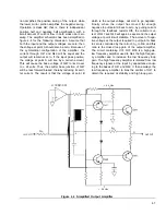
The main board schematic, sheet 2, shows the triangle
amplifier; it uses Q8, an FET source follower, to drive
Q10, a bipolar emitter follower, for an open loop gain
of one. It is a fast, very high input impedance circuit
with output impedance low enough to drive the hyster-
esis switch and the triangle buffer. In series with Q8 is
a matched duplicate FET, Q9. Q9 has the identical
drain current as Q8 and, therefore, the same gate-to-
source voltage. In series with Q10 is a duplicate emit-
ter follower, Q13. Q13 has the identical collector cur-
rent as Q10; therefore, it has the same emitter-to-
base voltage. Since the gate of the dummy FET, Q9, is
connected to the emitter of the dummy emitter
follower, Q13, the two terminals have the same
voltage. Therefore, within the tolerances of the part
parameters and some unaccounted error for base
current, the active emitter follower output voltage will
be at the value of the input gate. The remaining tran-
sistor, Qll, is a second emitter follower for driving the
dynamic lead networks at the input of the hysteresis
switch. In this role, it needs no dc integrity, as the out-
put is not directly coupled.
4.2.6
Hysteresis Switch
The hysteresis switch (main board schematic, sheet 2)
consists mainly of U14, a double input comparator,
and Q14/Q15, an output flip-flop. Each differential pair
of U14 compares an input voltage to common. The in-
put network provides a positive bias to one and a
negative bias to the other; therefore, when the input
terminal (output of the triangle amplifier) is at
1.25V,
the flip-flop changes state. The flip-flop selects which
input comparator of the hysteresis switch will be ac-
tivated in preparation for the next change of state.
When the timing capacitor is integrating positively,
the positive biased comparator is activated. When the
timing capacitor voltage r 1.25V, the flip-flop
changes state, the negative comparator is activated
and the direction of integration is reversed, so that
when the timing capacitor signal reaches - 1.25V,
the flip-flop switches back and the cycle starts over.
In addition to the positive and negative biases at the
comparator inputs, there is a dynamic lead network
on each one. These lead networks are driven by Q11,
a separate emitter follower, from the triangle ampli-
fier. They provide the necessary lead to compensate
for the inherent delays of the hysteresis switch,
thereby keeping the higher frequency dial nonlinearity
and sine distortion to a minimum.
4.2.7
Diode Gate and Timing Capacitor
The diode gate (current switch) and the timing
capacitor circuits are shown in the main board
schematic, sheet 2. The current source and sink are
switched to the timing capacitor by the hysteresis
switch via a diode bridge arrangement called the
diode gate. Actually, the hysteresis switch is linked to
the bridge network by two emitter followers, Q24 and
Q25, with independent outputs biased to be at the
4-5


