same voltage.
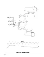
The simplified timing diagram il-
lustrated in figure 4-2 shows these points as one ter-
minal at C. When the hysteresis switch output is
positive, CR16 is forward biased, so that the current
sink is sourced by the drive circuit and is ineffective.
CR1 3 and CR1 5 are reverse biased, providing isolation
between the drive circuit and the timing capacitor.
This leaves CR14 forward biased and free to conduct
the current source output to the timing capacitor.
When the timing capacitor voltage rises to the hys-
teresis switch point (+ 1.25V), the hysteresis switch
output switches low, forward biasing CR13 which
back biases CR14 and CR16 and allows the source to
be isolated and the sink to discharge the timing capa-
citor through CR15 This state continues until the
negative switch point is reached and reverts to the
previous state.
diode network presenting a square wave input voltage
to the multiplier.
4.2.10
Transconductance Multiplier
After the main generator signal passes through the
function selector switch and the signal shaper circuit,
it enters a transconductance multiplier, U15 (main
board schematic, sheet 3), where the amplitude is set
by dc from the control amplifier or modulated by ac
from the modulation generator via the AM switch. Cur-
rents in the open collectors of this IC are worked into
a current mirror for optimum gain and fed to the pre-
amplifier summing node for conversion to a voltage
signal at TP7.
4.2.11 Preamplifier
4.2.8 Triangle Buffer
The triangle buffer (main board schematic, sheet 2) is
a wide band dc amplifier providing a closed loop gain
of one in potentiometric connection. The input dif-
ferential stage, Q17/Ql8, is a monolithic pair. The
emitters are fed from a current sink Q19. The active
collector load, Q20, is a current source providing
greater open loop gain than a resistive load. Following
this is an emitter follower, Q21, a zener diode level
shifter, CR1 2, and another emitter follower, Q22, for
t h e output stage. The gain is set to one by the 100%
feedback to the input pair feedback side, base of Ql8.
4.2.9 Signal Shaper
The signal shaper circuit (main board schematic,
sheet 3) is uniquely set’up for each different waveform
by four wafers of the function selector switch. The
15 volt power is switched off in the triangle wave
mode and there is virtually no effect on the triangle
wave fed to the circuit. In the positive pulse mode, the
square wave, rather than the triangle wave, is fed to
the circuit and the - 15 volt power is switched off. As
a result, the negative swing of the input square wave
is clipped off. The negative pulse is formed, when
selected by the function switch, in a similar manner.
When the square or sine wave is selected, both plus
and minus 15 volt power is applied to the circuit. The
difference in circuit setup for sine and square is the
resistive load at the circuit output and the shape of the
signal fed to the input. For the sine wave mode, the
matched set of -diodes soft clip the input triangle at
three different levels. These signals are resistively
summed to produce a sine wave voltage input to the
multiplier.
For the square wave mode, the input
square wave is symmetrically hard-clipped by the
The preamplifier (main board schematic, sheet 3), like
the output (power) amplifier, is comprised of a high
frequency ac amplifier combined with a low frequency
dc amplifier. It converts the current from the multiplier
to a voltage signal which is attenuated by the front
panel amplitude control and amplified by the output
amplifier. The U17 circuit is the dc amplifier and the
remaining circuitry is the high frequency amplifier.
Again, like the output amplifier, the ac amplifier is
symmetrically arranged from the R240/R238 summing
node to R246 and R249 at the output stage of the
preamplifier. If the input current goes into the node,
the voltage at the summing node will rise by a certain
amount. By capacitive coupling via C92 and C93, the
base voltage of Q40 rises closer to + 15 volts and the
base voltage of Q41 rises further away from - 15
volts. Thus, the emitter base junction of Q40 will be
less forward biased, thereby reducing the emitter cur-
rent, while the Q41 ‘emitter current increases. The
result is an increase in current in Q42 and a decrease
in current in Q43, causing a decreased voltage output
in R246/R249.The feedback path through R240 to the
summing node tends to cancel the rise in voltage
there, causing the output voltage to stabilize. T h e
amount of negative voltage at the output required to
pull the summing node back to zero is determined by
the value of R240.
4.2.12 Output
Amplifier
The output amplifier is comprised of a low frequency
dc amplifier and a high frequency ac amplifier. Refer
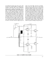
to the simplified circuit of figure 4-4. The U19, Q37
and Q38 circuit is the dc amplifier and the remaining
circuitry is the ac amplifier. The ac amplifier is sym-
metrically arranged, top and bottom. The upper por-
4-6


