English
INSTALLATION AND CONNECTION
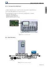
Indication of pins 1 e 2
GNDS
2 4 6
1
2
3
4
5
6
SP2
SP1
VINS
STO2
STO1
1 3 5
Figure 3.21:
XC2 connector location and pinout
Table 3.13:
XC2 connector (safety module)
XC2 connector
Pin
Name
Description:
(1)
1
GNDS
Safety module reference
2
VINS
+24 Vdc power supply for the safety module
3
SP2
Safety signal for STO2 input
4
STO2
Safety input 2
5
SP1
Safety signal for STO1 input
6
STO1
Safety input 1
(1)
For more information and connection examples, refer to the CFW900 safety
manual.
NF1
NA1
C1
NA2
C2
NA3
C3
F
N
1
2
3
4
5
6
7
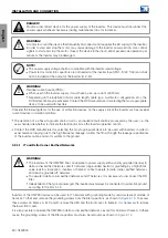
Figure 3.22:
CFW900-REL-01 XC30 connector pinout with example of AC load connection
Table 3.14:
XC30 connector (CFW900-REL-01 Accessory)
XC30 connector
Pin
Name
Description: Default Function (if any)
(1)
1
NF1
1A Digital Relay Output: No fault
(2)
NO: Normally Open, C: Common, NC:
Normally closed
2
NA1
3
C1
4
NA2
2A Digital Relay Output:
(2)
N>Nx ( S2.1.1 > C5.9.4)
5
C2
6
NA3
3A Digital Relay Output
(2)
N*>Nx ( S2.1.3 > C5.9.4)
7
C3
(1)
For more information see the detailed specification in Table 8.13.
(2)
The CFW900-REL-01 supplied with the inverter will be connected to slot A, and the
corresponding outputs will be 1A, 2A and 3A, with the default functions indicated. If the accessory
is reconnected to another slot, the identification of the outputs will change to 1n, 2n and 3n, with
‘n’ being the slot where the accessory was connected.
CFW900 | 41
Summary of Contents for CFW900
Page 2: ......


