


2–7
Operational Description
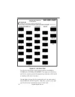
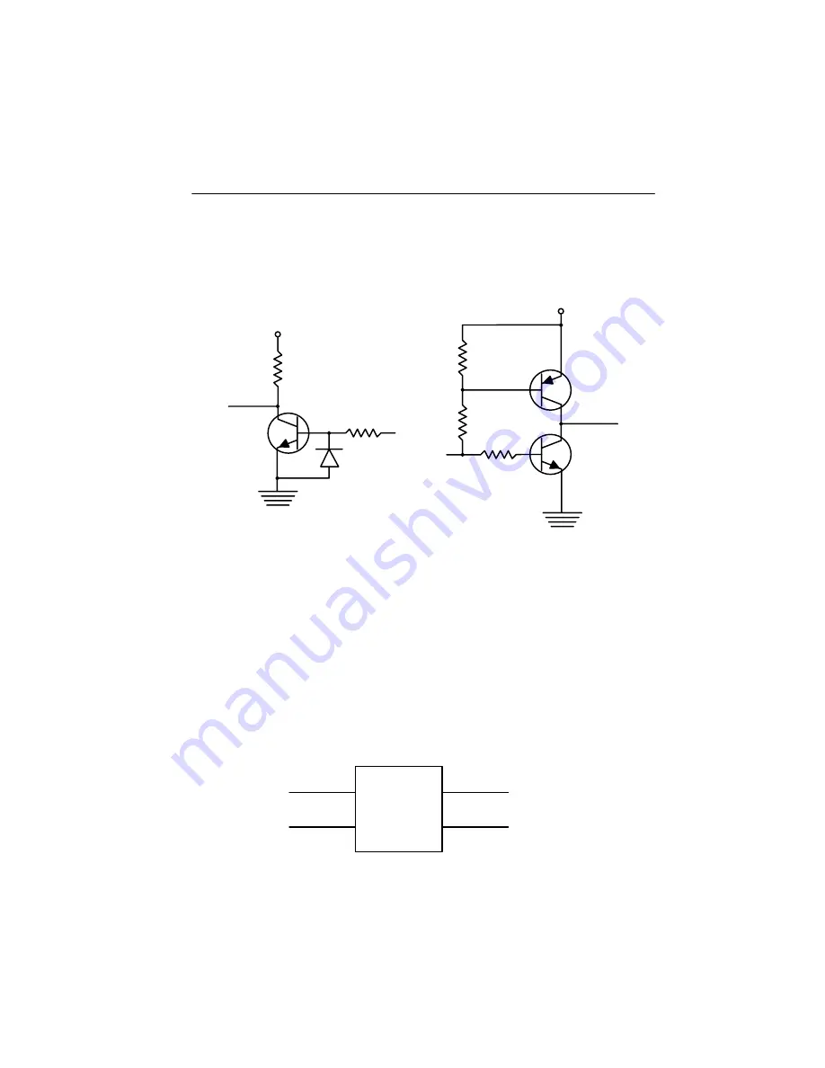
Schematic diagrams of the input and output circuits for the TTL logic
(Pseudo RS–232) are shown in Figure 2.1.
100K
R6
VCC
Q2
2N4401
D1
1N4148
R7
10K
R10
15K
VCC
Q3
2N4403
Q4
2N4401
R8
1K
R9
2.7K
Input Circuit
Output Circuit
Figure 2.3 SCANTEAM 6180 Input and Output Circuits
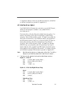
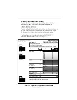
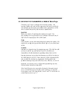
Schematic diagrams of the input and output circuits for the true RS–232
levels are shown in Figure 2.2. The operation of the DS1275 chip is
unique in that it “steals” current from the receive input when transmitting a
negative swing. Since most serial communications ports remain in a
negative state statically, using the receive signal for negative power greatly
reduces current consumption.
DS1275
TXD
RXD
TX
RX
Figure 2.4 SCANTEAM 6180 Input and Output Circuit
for the True RS–232 Scanner
Summary of Contents for Scanteam 6180
Page 1: ...Serial Interface RS 232 Decoded Out Wand Technical Manual ...
Page 2: ......
Page 6: ...Limited Warranty ...
Page 12: ...vi Table of Contents ...
Page 46: ...4 22 Programming the Scanner ...
Page 52: ...5 6 Maintenance and Troubleshooting ...
Page 65: ... ...
Page 66: ......
Page 67: ......