background image

2.20.3

Par al lel I/O VCC En able

The I/O con nec tors can pro vide +5 volts to an I/O rack or for mis cel la ne ous pur poses by jump er ing

J1. When J1 is ju5 volts is pro vided at pin 49 of  both J4 and J5. It the user's re spon si bil ity to
limit cur rent to a safe value (less than 1A) to avoid dam ag ing the CPU board.

2.20.4

WS16C48 Reg is ter Defi ni tions

The LBC- Plus uses the Win Sys tems’ ex clu sive ASIC de vice, the WS16C48. This de vice pro vides

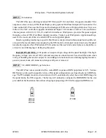
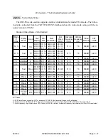
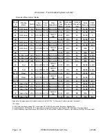
48 lines of  digi tal I/O. There are 17 unique reg is ters within the WS16C48. The fol low ing ta 

ble sum ma 

-

rizes the reg is ters and the text that fol lows pro vides de tails on each of the in ter nal reg is ters.

Page 2 - 22

OPERATIONS MANUAL LBC-Plus

991206

WinSystems - "The Embedded Systems Authority"

  1 o o 2
  3 o o 4
  5 o o 6
  7 o o 8
  9 o o 10
11 o o 12
13 o o 14
15 o o 16
17 o o 18
19 o o 20
21 o o 22
23 o o 24
25 o o 26
27 o o 28
29 o o 30
31 o o 32
33 o o 34
35 o o 36
37 o o 38
39 o o 40
41 o o 42
43 o o 44
45 o o 46
47 o o 48
49 o o 50

  1 o o 2
  3 o o 4
  5 o o 6
  7 o o 8
  9 o o 10
11 o o 12
13 o o 14
15 o o 16
17 o o 18
19 o o 20
21 o o 22
23 o o 24
25 o o 26
27 o o 28
29 o o 30
31 o o 32
33 o o 34
35 o o 36
37 o o 38
39 o o 40
41 o o 42
43 o o 44
45 o o 46
47 o o 48
49 o o 50

GND
GND
GND
GND
GND
GND
GND
GND
GND
GND
GND
GND
GND
GND
GND
GND
GND
GND
GND
GND
GND
GND
GND
GND
GND

GND
GND
GND
GND
GND
GND
GND
GND
GND
GND
GND
GND
GND
GND
GND
GND
GND
GND
GND
GND
GND
GND
GND
GND
GND

Port 2 Bit 7
Port 2 Bit 6
Port 2 Bit 5
Port 2 Bit 4
Port 2 Bit 3
Port 2 Bit 2
Port 2 Bit 1
Port 2 Bit 0
Port 1 Bit 7
Port 1 Bit 6
Port 1 Bit 5
Port 1 Bit 4
Port 1 Bit 3
Port 1 Bit 2
Port 1 Bit 1
Port 1 Bit 0
Port 0 Bit 7
Port 0 Bit 6
Port 0 Bit 5
Port 0 Bit 4
Port 0 Bit 3
Port 0 Bit 2
Port 0 Bit 1
Port 0 Bit 0

+5V

Port 5 Bit 7
Port 5 Bit 6
Port 5 Bit 5
Port 5 Bit 4
Port 5 Bit 3
Port 5 Bit 2
Port 5 Bit 1
Port 5 Bit 0
Port 4 Bit 7
Port 4 Bit 6
Port 4 Bit 5
Port 4 Bit 4
Port 4 Bit 3
Port 4 Bit 2
Port 4 Bit 1
Port 4 Bit 0
Port 3 Bit 7
Port 3 Bit 6
Port 3 Bit 5
Port 3 Bit 4
Port 3 Bit 3
Port 3 Bit 2
Port 3 Bit 1
Port 3 Bit 0

+5V

J4

J5

Summary of Contents for LBC- 486Plus

Page 1: ...OPERATIONS MANUAL LBC 486Plus LBC 586Plus WinSystems reserves the right to make changes in the circuitry and specifications at any time without notice Copyright 1997 by WinSystems All Rights Reserved ...

Page 2: ...ORY P N 403 0259 000 ECO Number Date Code Rev Level ORIGINATED 970422 C 97 36 970602 C1 97 78 970829 C2 97 105 971204 C3 98 01 980107 C4 98 18 980311 C5 98 57 980807 C6 98 86 980817 C7 99 30 990609 D 99 83 991206 E ...

Page 3: ... Bus Interface 2 14 2 13 Floppy Disk Interface 2 14 2 14 IDE Hard Disk Interface 2 16 2 15 Watchdog Timer Configuration 2 16 2 16 Status LED 2 17 2 17 Battery Select Control 2 17 2 18 Power Reset Connection 2 18 2 19 Silicon Disk Configuration 2 18 2 20 Parallel I O 2 21 2 21 VGA Configuration 2 24 2 22 Ethernet Configuration 2 29 2 23 Multi I O Connector 2 41 2 24 Jumper Connector Summary 2 42 3 ...

Page 4: ...ootable RAMDISK Usage 4 5 4 5 Non Bootable FLASHDISK Usage 4 7 4 6 DiskOnChip Usage 4 7 5 WS16C48 Programming Reference 5 1 Introduction 5 1 5 2 Function Definitions 5 1 5 3 Sample Programs 5 6 APPENDIX A I O Port Map APPENDIX B Interrupt Map APPENDIX C Parts Placement Guide APPENDIX D LBC Plus Mechanical Drawing APPENDIX E WS16C48 I O Routines and Sample Programs Listings WARRANTY ...

Page 5: ...y Parallel I O Four PC compatible serial ports are standard as are the floppy hard disk and parallel printer interfaces The LBC Plus is populated with either a 100 MHz AMD DX4 processor or the AMD 5x85 133 MHz processor Up to 32Mbytes of user installable SIMM memory is sup ported An optional 256KB level two cache is also available A full 16 bit PC 104 expansion bus is provided for further expansio...

Page 6: ...e or EDO DRAM in sizes from 1M to 32M SSD Memory Two 32 pin JEDEC standard sockets support 4 Mbit SRAM 4 Mbit PEROM 4 Mbit EPROM 8 Mbit EPROM or one M Systems 32 Pin DOC DiskOnChip module 1 3 3 Mechanical Dimensions 5 75 X 8 0 X 0 60 inches without PC 104 modules or cables PC Board FR4 Epoxy Glass with 4 signal layers and 2 power planes with screened component legend and plated through holes Jumpe...

Page 7: ...H 50 LP Power Reset 8 pin in line Molex PC 104 Bus 64 Pin SAMTEC type ESQ 132 12 G D 40 Pin SAMTEC type ESQ 120 12 G D 1 3 4 Environmental Operating Temperature 40 to 70 C Non condensing relative humidity 5 to 95 991206 OPERATIONS MANUAL LBC Plus Page 1 3 WinSystems The Embedded Systems Authority ...

Page 8: ...ell as the standard complement of AT class peripherals including 8 DMA Channels compatible with PC AT 8237A DMA controllers 15 interrupt inputs compatible with master slaved 8259 interrupt controllers Three 8254 compatible timer counter channels A PC AT compatible real time clock calendar with CMOS RAM A PCI BUS IDE interface A PC AT compatible keyboard interface These functional units are 100 PC ...

Page 9: ...FF 50 MHz OFF ON ON 66 MHz OFF ON OFF 80 MHz OFF OFF ON 100 MHz OFF OFF OFF NOTE The LBC Plus board will be jumpered at the factory for the rated speed of the installed processor Jumpering J12 to any speed in excess of the rated speed may result in CPU overheating misoperation and possible destruction of the CPU Failures of CPUs which have been operated above their rated speed or temperature are n...

Page 10: ... bit modules A single SIMM socket is provided which can support DRAM sizes from 1MB to 32MB Installation is accomplished with power off by angling the SIMM module approximately 30 de grees from vertical and inserting the fingers into the connector It may be necessary to remove any de viceinstalled intheU27socket TheSIMMmodule is keyed slightly off center andcannot beinserted backwards without extr...

Page 11: ...s The layout for the J30 header and the default jumper settings are shown here Page 2 4 OPERATIONS MANUAL LBC Plus 991206 WinSystems The Embedded Systems Authority 1 o o 2 3 o o 4 5 o o 6 7 o o 8 9 o o 10 11 o o 12 13 o o 14 15 o o 16 17 o o 18 19 o o 20 21 o o 22 J30 1 o o 2 3 o o 4 5 o o 6 7 o o 8 9 o o 10 11 o o 12 13 o o 14 15 o o 16 17 o o 18 19 o o 20 21 o o 22 J30 COM4 ENET COM3 COM4 WS16C4...

Page 12: ...rd Then remove the jumper from pins 1 2 on J13 and place on pins 2 3 for 30 seconds Replace the jumper on J13 pins 1 2 power up and reconfigure the CMOS settings as desired NOTE J13 is the master batteryenablejumper Removing the jumper removes battery powerfrom the entire board including the SSD array Be sure that any data contained in battery backed SRAM is backed up before removing the battery j...

Page 13: ...a the jumper block at J23 When J23 pins 1 2 are jumpered COM3 is enabled When J23 pins 3 4 are jumpered COM4 is enabled The interrupts are not disconnected when COM3 or COM4 are disabled Use the interrupt rout ing block described earlier to disconnect the default interrupts if desired Page 2 6 OPERATIONS MANUAL LBC Plus 991206 WinSystems The Embedded Systems Authority 1 2 3 o o o 1 2 3 o o o U9 U6...

Page 14: ...re 991206 OPERATIONS MANUAL LBC Plus Page 2 7 WinSystems The Embedded Systems Authority 1 2 3 o o o 1 2 3 o o o U3 Installed U4 Not Installed U8 Not Installed 1 o o 6 2 o o 7 3 o o 8 4 o o 9 5 o J8 J10 COM1 DB9 CD RX Data TX Data DTR GND DSR RTS CTS RI 1 2 3 o o o 1 2 3 o o o U5 Installed U6 Not Installed U9 Not Installed J9 J11 COM2 DB9 CD RX Data TX Data DTR GND DSR RTS CTS RI 1 o o 6 2 o o 7 3 ...

Page 15: ...ling resisters on the board in locations reserved for them The method for deter mining the correct resistor values is beyond the scope of this document but it is recommended that trial values of 100 ohms be used in all three locations at the receiver end The following illustration shows the correct mode jumpering driver IC installation I O connector pin definitions and termination resis tor locati...

Page 16: ... upon a number of factors including line imped ance line length etc A good trial value is 100 ohms in all three resistor locations The following illus trations show the correct jumpering driver IC installation I O connector pinout and termination resistor locations for each of the channels when used in RS 485 mode 991206 OPERATIONS MANUAL LBC Plus Page 2 9 WinSystems The Embedded Systems Authority...

Page 17: ...its transmitter enabled The transmitter Enable Dis able is controlled in software using bit 1 in the Mo dem Control Register RTS When RTS is set the transmitter is enabled and when cleared the normal state the transmitter is disabled and the receiver is enabled Note that it is necessary to allow some minimal settling time after enabling the transmitter before transmitting the first character Likew...

Page 18: ... 3 o o o 1 2 3 o o o U5 Not Installed U6 Installed U9 Not Installed 1 o o 6 2 o o 7 3 o o 8 4 o o 9 5 o J9 J11 COM2 DB9 N C TX RX TX RX N C GND N C N C N C N C VCC R14 R15 R16 TX RX TX RX RS 485 NOTE Because RS 485 uses a single twisted pair all transmitters are connected in paral lel Only one station at a time may transmit or have its transmitter enabled The transmitter Enable Dis able is control...

Page 19: ...o 9 5 o J8 J10 COM1 DB9 N C TX RX TX RX N C GND N C N C N C N C VCC R11 4 7K R12 Absent R13 4 7K TX RX TX RX R1 470 OHM R2 470 OHM C1 0022 ufd C2 0022 ufd 1 2 3 o o o 1 2 3 o o o U5 Not Installed U6 Installed U9 Not Installed 1 o o 6 2 o o 7 3 o o 8 4 o o 9 5 o J9 J11 COM2 DB9 N C TX RX TX RX N C GND N C N C N C N C VCC R14 4 7K R15 Absent R16 4 7K TX RX TX RX R5 470 OHM R4 470 OHM C4 0022 ufd C3 ...

Page 20: ...on The parallel port mode is selected via the jumper block at J6 per the following table J6 Jumpering SPP Mode EPP Mode ECP Mode EPP ECP Mode 3 5 4 6 3 5 2 4 1 3 4 6 1 3 2 4 991206 OPERATIONS MANUAL LBC Plus Page 2 13 WinSystems The Embedded Systems Authority 1 2 o o o o 3 4 1 2 o o o o 3 4 1 o o 2 3 o o 4 5 o o 6 J24 J21 J6 1 o o 14 2 o o 15 3 o o 16 4 o o 17 5 o o 18 6 o o 19 7 o o 20 8 o o 21 9...

Page 21: ...us supports up to 2 standard 3 1 2 or 5 1 4 PC compatible floppy disk drives The drives are connected via the I O connector at J17 Note that the interconnect cable to the drives is a stan dard floppy I O cable usedondesk top PCs The cable must have the twisted section prior to the drive A position The pin definitions for the J17 connector are shown here Page 2 14 OPERATIONS MANUAL LBC Plus 991206 ...

Page 22: ...GND MEMW MEMR IOW IOR DACK3 DRQ3 DACK1 DRQ1 REFRESH SYSCLK IRQ7 IRQ6 IRQ5 IRQ4 IRQ3 DACK2 TC BALE 5V OSC GND GND IOCHK BD7 BD6 BD5 BD4 BD3 BD2 BD1 BD0 IOCHRDY AEN SA19 SA18 SA17 SA16 SA15 SA14 SA13 SA12 SA11 SA10 SA9 SA8 SA7 SA6 SA5 SA4 SA3 SA2 SA1 SA0 GND C0 o o D0 C1 o o D1 C2 o o D2 C3 o o D3 C4 o o D4 C5 o o D5 C6 o o D6 C7 o o D7 C8 o o D8 C9 o o D9 C10 o o D10 C11 o o D11 C12 o o D12 C13 o o...

Page 23: ...The watchdog must be accessed every 1 5 seconds or a reset will occur Petting in this mode is accomplished by writing to I O port 1EFH with any value An alternate mode of operation is via software enable disable control This mode is set by jumper ing J19 pins 1 2 In this mode the watchdog timer powers up disabled and must be enabled in software before timing will begin Enabling is accomplished by ...

Page 24: ...aster batteryenablejumperis provided at J13 When J13 is jumpered pins 1 2 battery power is supplied to the Clock Calendar and to the individual jumper blocks for battery backup of SSD SRAMs When J13 is jumpered pins 2 3 the battery is totally disconnected and no current will be drawn from it Battery life is highly dependent upon duty cycle as there is no current drawn from the battery when 5 volts...

Page 25: ...his manual provides the necessary information for the generation and usage of the Silicon drives This section documents the re quired hardware configurations for the various type of devices Two 32 pin JEDEC memory sockets at U27 and U23 are used to contain the RAM ROM Flash or DOC devices used for the disk The silicon Page 2 18 OPERATIONS MANUAL LBC Plus 991206 WinSystems The Embedded Systems Auth...

Page 26: ...de with EPROMs RAMs of Flash devices installed effectively acts as a disable to the Solid State Disk and similarly when a DOC device is installed and the jumper is selected for standard devices the DOC is disabled IMPORTANT NOTE To insure Windows 95 compatibility J25 must be jumpered 1 2 2 19 2 Device Size Selection The onboard Solid State Disk array supports either 512K EPROMs SRAMs or FLASH devi...

Page 27: ...th EPROMs or PEROMs will result in the quick draining of the onboard battery 2 19 5 Silicon Disk Notes 1 When installing devices U27 is the first device in the array and must always contain the first de vice of a bootable disk 2 The DiskOnChip option must use the socket at U23 When a DOC is installed U27 is available as a Secondary Silicon Disk device See section 4 4 for more information Page 2 20...

Page 28: ... be enabled or disabled using the jumper block at J15 When J15 is jumpered the parallel I O is enabled at I O address 120H When J15 is open the 16 ad dresses starting at I O address 120H are free for use by other devices 2 20 2 Parallel I O Connectors The 48 lines of parallel I O are terminated through two 50 pin connectors at J4 and J5 The J4 con nector handles I O ports 0 2 while J5 handles port...

Page 29: ...3 o o 44 45 o o 46 47 o o 48 49 o o 50 1 o o 2 3 o o 4 5 o o 6 7 o o 8 9 o o 10 11 o o 12 13 o o 14 15 o o 16 17 o o 18 19 o o 20 21 o o 22 23 o o 24 25 o o 26 27 o o 28 29 o o 30 31 o o 32 33 o o 34 35 o o 36 37 o o 38 39 o o 40 41 o o 42 43 o o 44 45 o o 46 47 o o 48 49 o o 50 GND GND GND GND GND GND GND GND GND GND GND GND GND GND GND GND GND GND GND GND GND GND GND GND GND GND GND GND GND GND ...

Page 30: ...ternal10Kohmresistors Thisallowsit to be used as an input Whenused in the input mode a read reflects the inverted state of the I O pin such that a high on the pin will read as a 0 in the register Writing a 1 to a bit position causes the output pin to sink current up to 12mA effectively pulling it low INT_PENDING This read only register reflects the combined state of the INT_ID0 through INT_ID2 reg...

Page 31: ...s When set to a 1 the edge detection inter rupt is enabled for the corresponding port and bit When cleared to a 0 the bit s edge detection interrupt is disabled Note that this register can be used to individually clear a pending interrupt by disabling and reenabling the pending interrupt INT_ID0 INT_ID2 These registers are accessible when page 3 is selected They are used to identify currently pend...

Page 32: ...e is at the user s risk and extreme care should be ex ercised to avoid damaging or destroying the panel HAZARD WARNING LCD panels can require a high voltage for the panel backlight This high frequency voltage can exceed 1000 volts and can present a shock hazard Care should be taken when wiring or handling the inverter output To avoid danger of shock and to avoid damaging fragile and ex pensive pan...

Page 33: ...pecial controls that may be needed for the panel Refer to the FPA documentation for specific hook up instructions The pin definitions for J33 are shown here Page 2 26 OPERATIONS MANUAL LBC Plus 991206 WinSystems The Embedded Systems Authority 1 o o 2 3 o o 4 5 o o 6 7 o o 8 9 o o 10 RED GREEN BLUE HSYNC VSYNC GND GND GND GND GND J27 1 o o 2 3 o o 4 5 o o 6 7 o o 8 9 o o 10 11 o o 12 13 o o 14 15 o...

Page 34: ...X 200 25 175 31 5 70 256KB A B C 7 Text Mono 80 X25 80 X 25 80 X 25 9 X 16 9 X 14 9 X 8 720 X 400 720 X 350 720 X 350 28 322 31 5 70 256KB A B C D Planar 16 40 X 25 8 X 8 320 X 200 25 175 31 5 70 256KB A B C E Planar 16 80 X 25 8 X 8 640 X 200 25 175 31 5 70 256KB A B C F Planar Mono 80 X 25 8 X 14 640 X 350 25 175 31 5 70 256KB A B C 10 Planar 16 80 X 25 8 X 14 640 X 350 25 175 31 5 70 256KB A B ...

Page 35: ...0 30 5 68 256KB A B C 61 Text 16 132 X 50 8 X 16 1056 X 400 40 00 30 5 68 256KB A B C 6A 70 Planar 16 100 X 37 8 X 16 800 X 600 40 00 38 0 60 256KB B C 72 75 Planar 16 128 X 48 8 X 16 1024 X 768 65 00 48 5 60 512KB C 72 75I 44 90 35 5 43 512KB B C 78 Packed Pixel 16 80 X 25 8 X 16 640 X 400 25 175 31 5 70 256KB A B C 79 Packed Pixel 256 80 X 30 8 X 16 640 X 480 25 175 31 5 60 512KB A B C 7C Packed...

Page 36: ...tandards This functional block incorporates the receiver transmitter collision heartbeat loopback jabber and link integrity blocks as defined in the standard The transceiver when combined with the equaliza tion resistors transmit receive filters and pulse transformers provide a complete physical interface from the AT LANTIC Controller ENDEC module and the twisted pair medium The integrated ENDEC m...

Page 37: ... jumpers on J35 are ignored and the configuration information comes totally from the EEPROM Similarly if jumpered mode is selected the information in the EE PROM except for the Ethernet Address is ignored IMPORTANT NOTE Interrupts must ALWAYS be jumpered manually via the jumper block at J30 Section 1 6 which matches the jumpered or jumperless interrupt selection Page 2 30 OPERATIONS MANUAL LBC Plu...

Page 38: ... shown in the following illustrations 991206 OPERATIONS MANUAL LBC Plus Page 2 31 WinSystems The Embedded Systems Authority 11 o o 12 13 o o 14 15 o o 16 17 o o 18 19 o o 20 J35 11 o o 12 13 o o 14 15 o o 16 17 o o 18 19 o o 20 J35 11 o o 12 13 o o 14 15 o o 16 17 o o 18 19 o o 20 J35 11 o o 12 13 o o 14 15 o o 16 17 o o 18 19 o o 20 J35 11 o o 12 13 o o 14 15 o o 16 17 o o 18 19 o o 20 J35 11 o o...

Page 39: ...re shown here Page 2 32 OPERATIONS MANUAL LBC Plus 991206 WinSystems The Embedded Systems Authority 5 o o 6 7 o o 8 9 o o 10 11 o o 12 13 o o 14 J35 IRQ3 5 o o 6 7 o o 8 9 o o 10 11 o o 12 13 o o 14 J35 IRQ4 5 o o 6 7 o o 8 9 o o 10 11 o o 12 13 o o 14 J35 IRQ5 5 o o 6 7 o o 8 9 o o 10 11 o o 12 13 o o 14 J35 IRQ9 5 o o 6 7 o o 8 9 o o 10 11 o o 12 13 o o 14 J35 IRQ10 5 o o 6 7 o o 8 9 o o 10 11 o...

Page 40: ... T J22 Thin Ethernet Coax1 AUI2 J28 Twisted pair 10BASE T Reduced Squelch3 The J35 jumpering for each of the options is shown below 1 The thin Ethernet mode is not usable with the LBC Plus If thin Ethernet is required it is necessary to select the AUI mode and use an external transceiver 2 The AUI is connected via J28 An adapter cable WinSystems part number CBL 147 1 is avail able which terminates...

Page 41: ... supports the use of the remote boot feature available from NOVELL QNX and some other operating systems by allowing provisions for a user installed BIOS extension ROM into U23 Only a 27C010 EPROM device is supported in this mode although only 32K is available for the code If the BIOS extension is supplied in a smaller device it will have to be reprogrammed into a 27C010 device In order to use this...

Page 42: ...apters are recognized they will be displayed in a window on the right side of the screen as shown here From the main menu choose the desired function Each of the main menu options will be discussed in the following sections 991206 OPERATIONS MANUAL LBC Plus Page 2 35 WinSystems The Embedded Systems Authority WinSystems Thick Thin TPI August 20 1993 11 34PM PLUSCFG V1 17 AT LANTIC Configuration Sof...

Page 43: ...onoptions totheuser Theseinclude Adapter Architecture I O Port or Shared Memory Select Cable Interface Thin Ethernet or Thick Ethernet or 10BASE T The second prompt will only be present if there is no active cable attached or if the program is un able to determine the media type Page 2 36 OPERATIONS MANUAL LBC Plus 991206 WinSystems The Embedded Systems Authority WinSystems Thick Thin TPI August 2...

Page 44: ...ation as desired and then select Save Configuration to program the EEPROM with the new information NOTE PLUSCFG will not allow selection of I O ports interrupts or memory addresses that it be lieves are being used by other hardware in the system If PLUSCFG refuses to allow a desired selection for what you know are valid choices it will be necessary to use the jumpered mode described earlier for co...

Page 45: ...le at this time A sample screen is shown on the foll owing page Page 2 38 OPERATIONS MANUAL LBC Plus 991206 WinSystems The Embedded Systems Authority WinSystems Thick Thin TPI August 20 1993 11 34PM PLUSCFG V1 17 AT LANTIC Configuration Software AT LANTIC ADAPTERS I O Port Mode IRQ 0x320 I O Port 10 0x360 I O Port 5 CONFIGURATION INITIALIZATION AND DIAGNOSTICS Adapter Initialization disagnostics A...

Page 46: ...STICS Network Interface Controller 080017086050 OK Buffer Memory Check OK Check cable connection Cable Connected OK Interrupt Assignment 5 OK Boot Prom Check No Boot Prom OK Press ESC to return to previous menu Make Selection using arrow keys and enter Scroll through options using tab Make Selection using arrow keys and enter Scroll through options using tab AT LANTIC ADAPTERS I O Port Mode IRQ 0x...

Page 47: ...tems The Embedded Systems Authority AT LANTIC Configuration Software PLUSCFG V1 17 WinSystems Thick Thin TPI August 20 1993 11 34PM RECEIVED PACKET CONTENTS Received Status 01 Next Pointer 54 Receiver Length 1493 Destination 0040F698A3E6 Source 0040F6988448 Length Type 05C3 Hex HW CRC D703A649 SW CRC NORMAL 0450 98 7D D0 40 03 00 00 00 01 00 00 00 00 00 01 04 0460 51 33 33 87 02 01 00 00 00 04 00 ...

Page 48: ... o o 14 15 o o 16 17 o o 18 19 o o 20 21 o o 22 23 o o 24 25 o o 26 27 o o 28 29 o o 30 31 o o 32 33 o o 34 35 o o 36 37 o o 38 39 o o 40 41 o o 42 43 o o 44 45 o o 46 47 o o 48 49 o o 50 COM1 DCD COM1 RXD COM1 TXD COM1 DTR COM1 GND COM2 DSR COM2 RTS COM2 CTS COM2 RI LPT STROBE LPT PD0 LPT PD1 LPT PD2 LPT PD3 LPT PD4 LPT PD5 LPT PD6 LPT PD7 LPT ACK LPT BUSY LPT PE LPT SLCT KEYBD GND KEYBD KDATA KE...

Page 49: ...tor 2 16 J19 Watchdog timer configuration jumper 2 16 J20 VGA BIOS size select jumper 2 25 J21 ECP mode DMA select jumper 2 14 J22 10BASET I O connector N A J23 COM3 COM4 Enable Disable Select jumper 2 6 J24 ECP DMA select jumper 2 14 J25 SSD DOC Mode select jumper 2 19 J26 PC 104 8 connector 2 15 J27 Video output connector 2 26 J28 Ethernet AUI connector N A J29 PC 104 16 Connector 2 15 J30 Inter...

Page 50: ...nd you still wish to enter setup restart the system by turning it OFF and then ON or by pressing the RESET button if so equipped or by pressing the CTRL ALT and DEL key simultaneously Alter nately under certain error conditions of incorrect setup the message Press F1 to continue or DEL to Enter Setup may appear To Enter Setup at that time press the DEL key To attempt to continue ignoring the er ro...

Page 51: ...or the current month month the month JAN through DEC year The year from 1900 to 2099 Time The time is hour minute second The time is calculated on the 24 hour military time clock such that 1 00PM is 13 00 00 Page 3 2 OPERATIONS MANUAL LBC Plus 991206 WinSystems The Embedded Systems Authority ROM PCI ISA BIOS 2A4KD000 CMOS SETUP UTILITY AWARD SOFTWARE INC STANDARD CMOS SETUP PASSWORD SETTING BIOS F...

Page 52: ... 900 15 17 None 901 10 20 820 3 17 None 820 11 35 855 5 17 None 855 12 49 855 7 17 None 855 13 20 306 8 17 128 319 991206 OPERATIONS MANUAL LBC Plus Page 3 3 WinSystems The Embedded Systems Authority ROM PCI ISA BIOS 2A4KD000 STANDARD CMOS SETUP AWARD SOFTWARE INC Date mm dd yy Wed Sep 25 1996 Time hh mm ss 13 28 46 HARD DISKS TYPE SIZE CYLS HEAD PRECOMP LANDZ SECTOR MODE Primary Master Auto 0 0 0...

Page 53: ...24 14 17 None 1023 37 17 1024 2 17 None 1023 38 136 1024 16 17 None 1023 39 114 918 15 17 None 1023 40 40 820 6 17 None 820 41 42 1024 5 17 None 1023 42 65 1024 5 26 None 1023 43 40 809 6 17 None 852 44 61 809 6 26 None 852 45 100 776 8 33 None 775 46 203 684 16 38 None 685 Press PgUp or PgDn to select a numbered hard disk type or type the number and press ENTER Most manufacturers supply type info...

Page 54: ...E 360K 5 25 in 1 2M 5 25 in 720K 3 5 in 1 44M 3 5 in Video This category specifies the type of video adapter used for the primary system monitor that matches your video display board and monitor The available choices are EGA VGA CGA40 CGA80 MONO The LBC Plus has built in VGA support so EGA VGA should be selected Error Halt This category determines whether the system will halt if a non fatal error ...

Page 55: ...that can be used for different applications DOS may use this area to load device drivers and TSRs to keep as much base memory free as possible for application programs The most common use of this area is for shadow RAM 3 5 Bios Features Setup Virus Warning This option when enabled protects the boot sector and partition table of the hard disk against unau thorized writes through the BIOS Any attemp...

Page 56: ...r 80 tracks If disabled no seek test will be performed and no error can be reported 991206 OPERATIONS MANUAL LBC Plus Page 3 7 WinSystems The Embedded Systems Authority ROM PCI ISA BIOS 2A4KD000 BIOS FEATURES SETUP AWARD SOFTWARE INC Virus Warning Disabled Video BIOS Shadow Enabled CPU Internal Cache Enabled C8000 CFFFF Shadow Enabled External Cache Enabled D0000 D7FFF Shadow Disabled Quick Power ...

Page 57: ...ipset Typematic Rate Setting This option enables or disables the typematic rate programming at boot time Typematic is the auto repeat function for the keyboard Typematic Rate When the typematic rate setting is enabled the typematic repeat speed is set via this option The sup ported rates are 6 characters per second 8 characters per second 10 characters per second 12 characters per second 15 charac...

Page 58: ...r a particular address range is enabled it instructs the BIOS to copy the BIOS located in ROM into DRAM This shadowing from an 8 bit EPROM into fast 32 bit DRAM results in a Multi magnitude increase in performance The main BIOS is shadowed automatically but there are other areas that may be selected for shadowing as shown here Video BIOS Shadow C000 C7FFF EGA VGA BIOS ROM C8000 CFFFF D0000 D7FFF D...

Page 59: ...ration If the system works well enough to get into Setup simply choose the Load BIOS Defaults option and then select Save and Exit Setup to restore factory defaults If the system will not run well enough to run Setup it will be necessary to remove the battery source temporarily until the CMOS memory decays Refer to Section 2 X for details on reinitializing the CMOS RAM Each of the options for the ...

Page 60: ...al default fast fastest 991206 OPERATIONS MANUAL LBC Plus Page 3 11 WinSystems The Embedded Systems Authority ROM PCI ISA BIOS 2A4KD000 CHIPSET FEATURES SETUP AWARD SOFTWARE INC Auto Configuration Enabled AT BUS Clock CLK 4 DRAM Read Timing Normal DRAM Write Timing Normal SRAM Read Timing 3 1 1 1 SRAM Write Timing 0 Wait ISA I O Recovery Disabled Fast Back to Back Disabled On Chip Local Bus IDE En...

Page 61: ...ns The choices are 0 Wait 1 Wait Default ISA I O Recovery The CPU and local bus are much faster than the standard for the ISA bus Selecting enabled for this option allows additional time for I O devices to respond to the system The default is disabled Fast Back To Back When enabled consecutive write cycles targeted to the same slave become fast back to back on the PCI bus The default setting is di...

Page 62: ...cting Auto will allow the BIOS to automatically select the optimum transfer mode for the master hard disk The default set ting is Auto IDE Primary Slave PIO Like the previous item this option allows for the selection of any one of 5 IDE transfer modes or an Auto selection which allows the BIOS to auto optimize the IDE transfers to from the slave hard disk The default setting is Auto 3 7 Load BIOS ...

Page 63: ...tential by interrogat ing the driver as to its preferred configuration of tracks heads and sectors and automatically loading these parameters into a user defined hard disk type 3 11 Save Exit Setup This function writes all changes to CMOS RAM and restarts the system 3 12 Exit without Saving This option exits setup without saving any changes made and then restarts the system Page 3 14 OPERATIONS MA...

Page 64: ...s of up to 1 Megabyte may be used as the boot media Onboard support is provided for the formatting reading and writing of the Floppy drive emulating PEROMs 3 For Applications needing to log data update the application or for convenience during develop ment battery backed SRAM may be used as the boot media with a size of up to 1 Megabyte 4 The LBC Plus supports the M Systems Disk On Chip Devices DO...

Page 65: ...your selection MKDISK Main Menu MKDISK Solid State RomDisk Creation Utility V6 00 C 1988 1994 WinSystems Inc SELECT SOURCE DISK TYPE 160 KB 5 1 4 Single Sided 8 Sectors 40 tracks 180 KB 5 1 4 Single Sided 9 Sectors 40 tracks 320 KB 5 1 4 Double Sided 8 Sectors 40 tracks 360 KB 5 1 4 Double Sided 9 Sectors 40 tracks 720 KB 3 1 2 Double Sided 9 Sectors 80 tracks 720 KB 5 1 4 Double Sided 9 Sectors 8...

Page 66: ...MANUAL LBC Plus Page 4 3 MKDISK Solid State RomDisk Creation Utility V6 00 C 1988 1994 WinSystems Inc SELECT SOURCE DRIVE Drive A Drive B Use arrow keys and ENTER to make your selection MKDISK Drive Menu MKDISK Solid State RomDisk Creation Utility V6 00 C 1988 1994 WinSystems Inc SELECT ROM SIZE 32K X 8 ROM 27C256 type 64K X 8 ROM 27C512 type 128K X 8 ROM 27C010 type 256K X 8 ROM 27C020 type 512K ...

Page 67: ...s supports bootable RAMDISKs and FLASHDISKs of up to 1 Megabyte in size 512K X 8 Static RAMs PEROMs can be installed in the board beginning at U27 One or two RAMs PEROMs can be installed and the device jumpers should be appropriately set as described in section 2 20 After powerup it is necessary to configure the silicon disk for the actual size of the drive using the SSDINIT utility SSDINIT is inv...

Page 68: ...n and will wear out with excessive write cycles ATMEL specifies at least 10 000 write cycles 4 4 Non Bootable RAMDISK Usage A non bootable RAMDISK is often desired in conjunction with a bootable ROMDISK FLASH DISK or rotational media It can then be used for program updates parameter storage or data logging applications a non bootable RAMDISK uses the WinSystems Universal Solid State Disk Driver US...

Page 69: ...he follow ing CONFIG SYS command line device ussd sys mod p seg e000 psz 16 inc 1 pad 1ec spg 80 dsz 512 this will create a 512K RAMDISK in the silicon disk socket U27 NOTE USSD as is the convention with DOS installable disk devices creates a drive with the NEXT AVAILABLE drive letter Drives A and B are always reserved for the physical floppy drive or the BIOS supported bootable Silicon Disk In a ...

Page 70: ...MB to 12MB The DOC device contains a BIOS extension the TFFS Tiny Flash File System and the Flash memory all in a single 32 pin device The DOC unlike the other WinSystems SSD support for the LBC Plus emulates a hard disk rather than a floppy disk The DOC can be used as a secondary hard disk to a physical IDE drive or it can be the only hard disk in the system The DOC is installed into the socket a...

Page 71: ...should include the header file uio48 h which includes the function prototypes and the needed con stant definitions Note that all of the functions utilize the concept of bit_number The bit_number is a value from 1 to 48 1 to 24 for interrupt related functions that correlates to a specific I O pin Bit_number 1 is port 0 bit 0 and continues through to bit_number 48 at port 5 bit 7 INIT_IO Initialize ...

Page 72: ...he pin is high WRITE_BIT Write a 1 or 0 to an I O pin Syntax void write_bit int bit_number int value Description This function takes two arguments bit_number This is value from 1 to 48 which is the bit to be acted upon Value is either 1 or 0 This function allows for writing of a single bit to either a 0 or a 1 as specified by the second argu ment There is no return value and other bits in the I O ...

Page 73: ...eturn value and other bits in the same I O port are unaffected CLR_BIT Clear the specified I O Bit Syntax void clr_bit int bit_number Description This function takes a single argument bit_number a value from 1 to 48 indicates the bit number to clear This function clears the specified I O bit Note that clearing the I O bit results in the actual I O pin going high This function does not affect any b...

Page 74: ...roller install vectors or handle interrupts when they occur There is no return value and only the specified bit is affected DISAB_INT Disable Edge Detect Interrupt Detection Syntax void disab_int int bit_number Description This function requires a single argument bit_number A value from 1 to 24 specifying the appropriate bit This function shuts down the edge detection interrupts for the specified ...

Page 75: ...ling this function with no inter rupt pending will have no adverse affect Only the specified bit is affected GET_INT Retrieve bit number of pending interrupt Syntax int get_int void Description This function requires no arguments and returns either a 0 for no bit interrupts pending or a value between 1 and 24 representing a bit number that has a pending edge detect interrupt The function re turns ...

Page 76: ... additional features of the WS16C48 and the I O library functions It pro grams the first 24 bits for input arms them for falling edge detection and then polls using the library routine get_int to determine if any transitions have taken place INT C This program was compiled with Borland C C version 3 1 on the command line with bcc int c uio48 c This program is identical in function to the poll c pr...

Page 77: ...pset Registers 024 03F FREE 040 043 8254 Timer 044 05F FREE 060 06F 8042 Keyboard Controller 070 071 CMOS RAM RTC 072 07F FREE 080 08F DMA Page Registers 090 09F FREE 0A0 0BF 8259 PIC 2 0C0 0DF 8237 DMA 2 0E0 0EF FREE 0F0 0F1 Coprocessor Control 0F2 11F FREE 120 12F WS16C48 HDIO 130 1DF FREE 1E0 1EF SSD Led Watchdog control 1F0 1FF Fixed Disk I O 200 20F Joystick port 210 21F PCM SSD I O Ports 220...

Page 78: ... 3B0 3BB DMA 3C0 3CF EGA 3E8 3EF COM3 3F0 3F6 Floppy Disk 3F8 3FF COM1 Page 6 2 OPERATIONS MANUAL LBC Plus 991206 WinSystems The Embedded Systems Authority ...

Page 79: ...on D 34 Hardware IRQ5 XT Hard Disk AT Free 286 Protection fault exception E 38 Hardware IRQ6 Floppy Disk Interrupt 386 Page fault exception F 3C Hardware IRQ7 LPT1 10 40 BIOS Video BIOS functions 286 Coprocessor exception 11 44 BIOS BIOS Equipment check 486 Alignment check exception 12 48 BIOS Memory Size function 13 4C BIOS BIOS Disk functions 14 50 BIOS BIOS serial functions 15 54 BIOS Cassette ...

Page 80: ...xed disk 1 parameter table 42 108 BIOS EGA Chain 43 10C BIOS EGA Parameter table pointer 44 110 BIOS EGA graphics character font 4A 128 BIOS AT Alarm exit address 50 140 BIOS AT Alarm interrupt 51 144 BIOS Mouse functions 5A 168 NET Functions 5B 16C NET Boot chain 5C 170 NET Net BIOS entry 67 19C MS DOS EMS functions 6D 1B4 VGA VGA Service 70 1C0 Hardware IRQ8 Real Time clock 71 1C4 Hardware IRQ9 ...

Page 81: ...8 APPENDIX C LBC Plus Parts Placement Guide Top 991206 OPERATIONS MANUAL LBC Plus Page 8 1 ...

Page 82: ...LBC Plus Parts Placement Guide Bottom Page 8 2 OPERATIONS MANUAL LBC Plus 991206 WinSystems The Embedded Systems Authority ...

Page 83: ...9 APPENDIX D LBC PLUS Mechanical Drawing ...

Page 84: ......

Page 85: ...10 APPENDIX E WS16C48 I O Routines and Sample Program Listings ...

Page 86: ...r implied In no case shall WinSystems be liable for any direct or indirect loss or damage real or consequential resulting from the usage of this source code It is the user s sole responsibility to determine fitness for any considered purpose Name uio48 h Project PCM UIO48 Software Samples Examples Date October 30 1996 Revision 1 00 Author Steve Mottin Changes Date Revision Description ________ ___...

Page 87: ... Changes Date Revision Description ________ ________ ______________________________________________ 10 30 96 1 00 Created include dos h This global holds the base address of the UIO chip unsigned base_port This global array holds the image values of the last write to each I O ports This allows bit manipulation routines to work without having to actually do a read modify write to the I O port unsig...

Page 88: ... takes two arguments bit_number The I O pin to access is specified by bit_number 1 to 48 val The setting for the specified bit either 1 or 0 This function sets the specified I O pin to either high or low as dictated by the val argument A non zero value for val sets the bit void write_bit int bit_number int val unsigned port unsigned temp unsigned mask Adjust bit_number for 0 based numbering bit_nu...

Page 89: ... the interrupt on the flling edge This function enables within the 16C48 an interrupt for the specified bit at the specified polarity This function does not setup the interrupt controller nor does it supply an interrupr handler void enab_int int bit_number int polarity unsigned port unsigned temp unsigned mask Adjust for 0 based numbering bit_number Calculate the I O address based uppon the bit nu...

Page 90: ... Calculate the I O Address for the enable port port bit_number 8 base_port 8 Calculate the proper bit mask for this bit number mask 1 bit_number 8 Turn on access to page 2 registers outportb base_port 7 0x80 Get the current state of the enable register temp inportb port Clear the enable bit int the image for our bit number temp temp mask Update the enable register with the new information outportb...

Page 91: ...pt currently pending Range is 1 to 24 This function returns the highest level interrupt pending If no interrupt is pending a zero is returned This function does NOT clear the interrupt int get_int void int temp int x read the master interrupt pending register mask off undefined bits temp inportb base_port 6 0x07 If there are no interrupts pending return a 0 if temp 7 0 return 0 There is something ...

Page 92: ...0x0a Read port 2 status If any pending return the appropriate bit number if temp 0 for x 0 x 7 x if temp 1 x outportb base_port 7 0 Turn off access return x 17 Return bitnumber with active int We should never get here unless the hardware is misbehaving but just to be sure We ll turn the page access back to 0 and return a 0 for no interrupt found outportb base_port 7 0 return 0 ...

Page 93: ...resulting from the usage of this source code It is the user s sole responsibility to determine fitness for any considered purpose include stdio h include conio h include dos h include uio48 h This is where we have our board jumpered to define BASE_PORT 0x200 This is an utlra simple demonstration program of some of the functions available in the UIO48 source code library This program simply sets an...

Page 94: ... h include conio h include uio48 h define BASE_PORT 0x200 This program uses the edge detection interrupt capability of the WS16C48 to count transitions on the first 24 lines It does this however no by using true interrupts but by polling for transitions using the get_int function Our transition totals are stored in this array unsigned int_counts 25 Definitions for local functions void check_ints v...

Page 95: ...r of a pending transition interrupt current get_int If it s 0 there are none pending if current 0 return Clear and rearm this one so we can get it again clr_int current Tally a transition for this bit int_counts current ...

Page 96: ...WS16C48 to count edge transitions Unlike poll c however this program actually uses interrupts and update all of the transition counters in the background Our transition totals are stored in this global array unsigned int_counts 25 Function declarations for local functions void check_ints void void interrupt int_handler void void interrupt old_handler void void main int x Initialize the I O ports S...

Page 97: ...ed enable This function is executed when an edge detection interrupt occurs void interrupt int_handler void int current Get the current interrupt pending There really should be one here or we shouldn t even be executing this function current get_int We will continue processing pending edge detect interrupts until there are no more present In which case current 0 while current Clear the current one...

Page 98: ...REIN THERE ARE NO OTHER WARRANTIES EXPRESS OR IMPLIED INCLUDING BUT NOT LIMITED TO THE IMPLIED WARRANTIES OF MERCHANTABILITY AND FITNESS FOR A PARTICULAR PURPOSE IN NO EVENT SHALL WINSYSTEMS BE LIABLE FOR CONSEQUENTIAL INCIDENTAL OR SPECIAL DAMAGES INCLUDING BUT NOT LIMITED TO DAMAGES FOR LOSS OF DATA PROFITS OR GOODWILL WINSYSTEMS MAXIMUM LIABILITY FOR ANY BREACH OF THIS AGREEMENT OR OTHER CLAIM ...

Reviews: