


• Elements for ESD protection should be placed on all pins that are accessible from the
outside and should be placed close to the accessible area. For example, the RF-pin is
accessible when using an external antenna and should be protected.
• ESD protection for the antenna connection must be chosen such as to have a minimum
effect on the RF signal. For example, a protection diode with low capacitance such as
the 8231606A or a 68 nH air-core coil connecting the RF-line to ground give good
results.
• Placeholders for optional antenna matching or additional filtering are recommended.
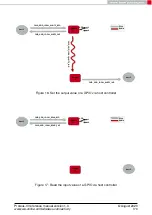
• The antenna path should be kept as short as possible.
Again, no fixed values can be recommended, as they depend on the influenc-
ing circumstances of the application (antenna, interferences etc.).
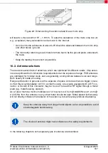
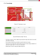
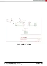
Figure 20: Layout
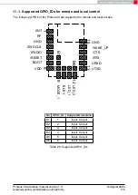
• To avoid the risk of short circuits and interference there should be no routing under-
neath the module on the top layer of the baseboard.
• On the second layer, a ground plane is recommended, to provide good grounding and
shielding to any following layers and application environment.
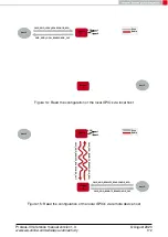
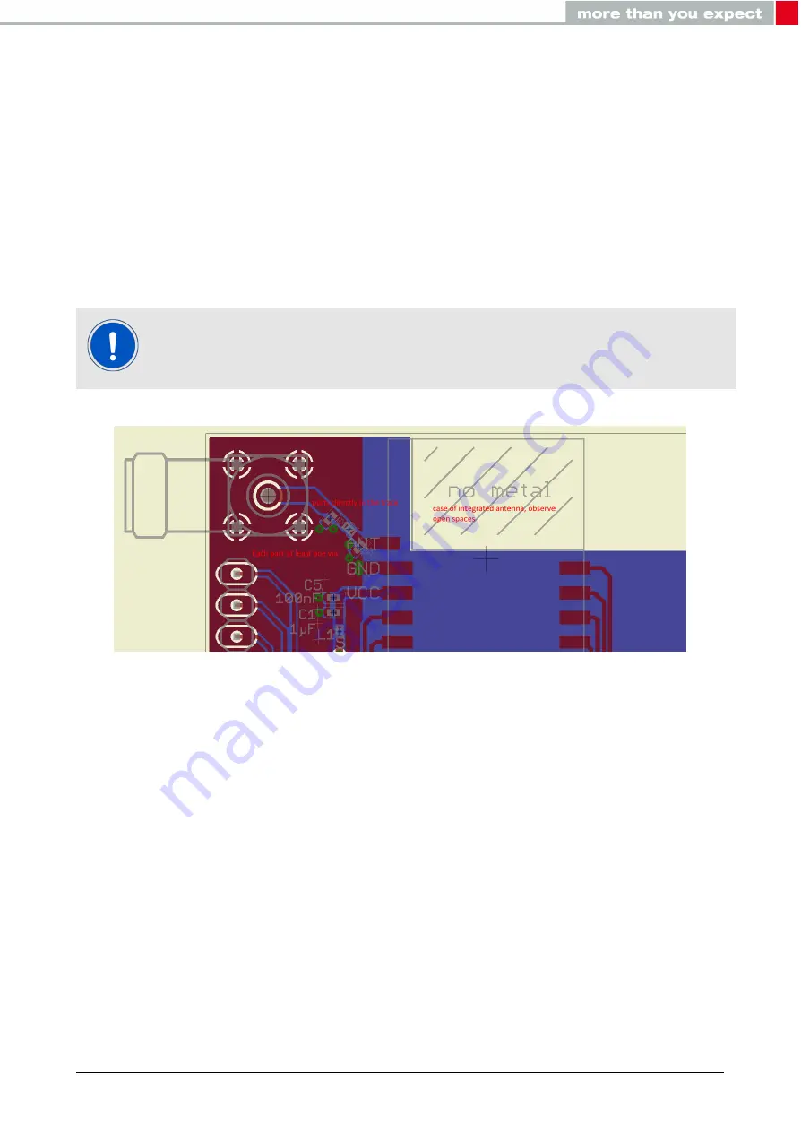
• In case of integrated antennas it is required to have areas free from ground. This area
should be copied from the evaluation board.
• The area with the integrated antenna must overlap with the carrier board and should
not protrude, as it is matched to sitting directly on top of a PCB.
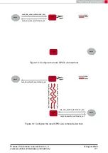
• Modules with integrated antennas should be placed with the antenna at the edge of
the main board. It should not be placed in the middle of the main board or far away
from the edge. This is to avoid tracks beside the antenna.
Proteus-III reference manual version 1.3
© August 2020
www.we-online.com/wireless-connectivity
185


