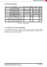
2.5. Pin characteristics
Property
Min
Typ.
Max
Unit
RF Pin input voltage
2.1
V
GPIO Voltage Input high
0.65
×
VCC
VCC
V
GPIO Voltage Input low
-0.5
0.35
×
VCC
V
GPIO Voltage Output high
0.8
×
VCC
VCC
V
GPIO Voltage Output low
0
0.2
×
VCC
V
/RESET
Voltage Input low
0.6
V
Pin output current sunk by any I/O and
control pin, drive mode dependant
2
mA
Pin output current sourced by any I/O and
control pin, drive mode dependant
2
mA
Table 7: Pin characteristics
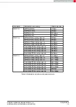
2.6. TX power vs current consumption
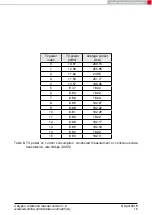
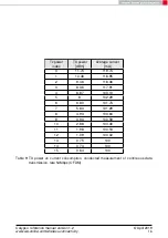
The following tables contains the typical TX power values and the corresponding typical
average current for 3.6V supply voltage and 25°C ambient temperature. Cable loses of the
conducted measurement are about 2dB.
Calypso reference manual version 1.2
© April 2019
www.we-online.com/wireless-connectivity
14

