background image

RELEASE DATE: 9/11/1999

XSV Board V0.1 Manual

XSV Board V0.1 Manual

How to install and use
your new XSV Board

2608 Sweetgum Drive

Apex NC 27502

Toll-free: 800-549-9377

International: 919-387-0076

FAX: 919-387-1302

Summary of Contents for XSV

Page 1: ...SE DATE 9 11 1999 XSV Board V0 1 Manual XSV Board V0 1 Manual How to install and use your new XSV Board 2608 Sweetgum Drive Apex NC 27502 Toll free 800 549 9377 International 919 387 0076 FAX 919 387...

Page 2: ...sion Subject to the limitations specified above your sole and exclusive warranty shall be during the period of warranty specified above and at XESS s option the repair or replacement of the product Th...

Page 3: ...ng to a PC 8 Setting the Oscillator Frequency 8 Programming the Interface 10 Downloading Virtex Configuration Bitstreams 10 XSV Circuitry 11 Programmable logic XCV50 XCV800 Virtex FPGA and XC95108 CPL...

Page 4: ...3 Digit and Bargraph LEDs 24 PS 2 Port 26 Dual USB Port 26 Parallel Port 27 Serial Port 29 Xchecker Cable 29 Power Connectors 30 XSV Pin Connections 31 XSV Schematics 33...

Page 5: ...com or check our web site at http www xess com n If you can t get your XILINX software tools installed properly send an e mail message describing your problem to hotline xilinx com or check their web...

Page 6: ...re the XSV Board through a PC parallel port serial port Xchecker cable or from a bitstream stored in the 16 Mbit Flash RAM The Flash RAM can also store data for use by the FPGA after configuration is...

Page 7: ...graph let the FPGA and CPLD display status information n Mouse keyboard PS 2 port gives the FPGA access to common PC input devices n Dual USB port provides the FPGA with two independent serial I O cha...

Page 8: ...7...

Page 9: ...PC One DB25 connector on the 6 foot cable should be attached to connector J10 on the XSV Board and the other end should plug into the parallel port connector of a PC Setting the Oscillator Frequency T...

Page 10: ...quency should now be 100 MHz DIVISOR You can substitute an external clock source for the internal oscillator Follow these steps to configure the programmable oscillator for operation with an external...

Page 11: ...ce a shunt on jumper J23 q Restore power to the XSV Board q Reconnect the cable to the PC parallel port q Enter the following command in a DOS window if you want to program the XSV Board through the P...

Page 12: ...llator A Dallas DS1075 programmable oscillator provides a clock signal to both the FPGA and the CPLD The DS1075 has a maximum frequency of 100 MHz which can be divided to provide frequencies of 100 MH...

Page 13: ...tream whenever the XSV Board is powered up After power up the FPGA can read and or write the Flash Of course the CPLD and FPGA have to be programmed such that they do not conflict if both are trying t...

Page 14: ...D0 177 32 D1 167 33 D2 163 34 D3 156 35 D4 145 36 D5 138 37 D6 134 39 D7 124 40 A0 132 16 A1 133 17 A2 139 18 A3 141 19 A4 144 20 A5 147 23 A6 152 24 A7 154 25 A8 157 27 A9 160 28 A10 162 29 A11 169...

Page 15: ...x FPGA Pin to Left Bank Virtex FPGA Pin to Right Bank CE 186 109 OE 228 95 WE 201 68 D0 202 70 D1 203 71 D2 205 72 D3 206 73 D4 207 74 D5 208 78 D6 209 79 D7 215 80 D8 216 81 D9 217 82 D10 218 84 D11...

Page 16: ...CAM and PAL video signals using the SAA7113 video decoder The digitized video arrives at the FPGA over the VPO bus The arrival of video data is synchronized with the rising edge of the LLC line locked...

Page 17: ...imple resistor ladder DAC The outputs of the DAC are sent to a VGA monitor along with the horizontal and vertical sync pulses HSYNC VSYNC from the FPGA When the RAMDAC generates the VGA color signals...

Page 18: ...placement to enable the FPGA to generate VGA signals directly or through the RAMDAC is shown below J7 J7 J5 J5 J6 J6 Direct VGA Shunt Setting RAMDAC Shunt Setting The pin assignments for the connecti...

Page 19: ...LRCK signal to select the left or right channel as the source destination of the serial data The master clock from the FPGA MCLK synchronizes all the internal operations of the codec The FPGA pins wh...

Page 20: ...static values on pins which control the configuration of the PHY chip Pins MF0 4 set the modes for auto negotiation repeating symbol transmission scrambling etc Likewise the configurations signals CFG...

Page 21: ...ed for data transmission and reception and are usually only active after system initialization LXT970A Pin Virtex FPGA Pin XC95108 CPLD Pin RAMDAC COL 23 CRS 21 TRSTE 24 TX_CLK 210 TX_EN 25 TX_ER 27 T...

Page 22: ...the left and right expansion headers are also connected to the left and right banks of SRAM respectively The SRAM bank chip enable should be raised to disable the SRAMs on that side if the associated...

Page 23: ...E 17 202 70 D0 18 203 71 D1 19 5 20 205 72 D2 21 206 73 D3 22 207 74 D4 23 GND 24 208 78 D5 25 209 79 D6 26 215 80 D7 27 3 3 28 216 81 D8 29 217 82 D9 30 218 84 D10 31 GND 32 220 85 D11 33 221 86 D12...

Page 24: ...open or OFF the pin is pulled high through a resistor When not being used the DIP switches should be left in the open or OFF configuration so the pins of the FPGA and CPLD are not tied to ground and...

Page 25: ...and two more 7 segment LED digits for use by the FPGA and CPLD All of these LEDs are active high meaning that an LED segment will glow when a logic high is applied to it The table below lists the con...

Page 26: ...8 37 D5 Left Digit SL6 134 39 D6 SR0 124 40 D7 SR1 132 16 A0 SR2 133 17 A1 SR3 139 18 A2 SR4 141 19 A3 SR5 144 20 A4 Right Digit SR6 147 23 A5 B0 152 24 A6 B1 154 25 A7 B2 157 27 A8 B3 160 28 A9 B4 16...

Page 27: ...ta stream that is synchronized with the falling edges on the clock signal The following table shows the connections from the FPGA to the PS 2 interface PS 2 Port Pin Virtex FPGA Pin CLK 13 DATA 17 Dua...

Page 28: ...of the FPGA to the USB ports are listed below Dual USB Port Pin Virtex FPGA Pin D 9 Lower Port D 10 D 11 Upper Port D 12 Parallel Port The CPLD handles the interface to the parallel port The seventeen...

Page 29: ...stor prevents the TDO output from interfering with the general purpose I O pin during routine parallel port operations The table below lists the connections from the parallel port to the general purpo...

Page 30: ...0 Xchecker Cable Header J21 provides an interface between the FPGA and an Xchecker cable The Xchecker cable can be used to perform configuration and readback operations on the FPGA Xchecker Pin Virtex...

Page 31: ...he XSV Board through connector J11 The connector is keyed so power cannot be applied with the wrong polarity The XSV Board can also be powered from a 9 VDC power supply through jack J12 The power supp...

Page 32: ...write SW4 32 Df0 Sl0 57 5V 82 RTS 8 cs 33 Df1 Sl1 tdi 58 Af19 DIPSW7 83 TDO 9 init 34 Df2 Sl2 tdo 59 Af20 DIPSW8 84 GND 10 done 35 Df3 Sl3 tms 60 LP13 85 CTS 11 program 36 Df4 Sl4 61 LP12 86 MF4 12 c...

Page 33: ...5V 208 Dl5 29 GND 89 DS1075 CLKI 149 Af17 DIPSW5 209 Dl6 30 3 3V 90 3 3V 150 210 TxCLK 31 TxD4 RS0 91 GND 151 GND 211 GND 32 2 5V 92 LLCK 152 Af6 B0 212 3 3V 33 RxD4 93 Dr14 153 Af16 DIPSW4 213 RxCLK...

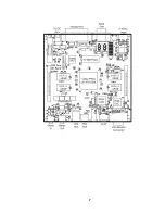
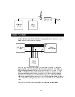
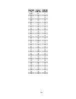
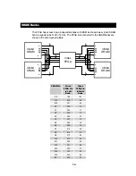
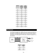
Page 34: ...33 B XSV Schematics The following pages show the detailed schematics for the XSV Board...

Page 35: ......

Page 36: ......

Page 37: ......

Page 38: ......

Page 39: ......

Page 40: ......

Page 41: ......

Page 42: ......

Page 43: ......

Page 44: ......

Page 45: ......

Page 46: ......

Page 47: ......

Page 48: ......

Page 49: ......

Page 50: ...XSV Board V0 1 Layout...

Reviews: