background image


XIIMUS R-GB-IR CL User Manual.                                            Version 1.2


4. 

PROCESSING OF CCD OUTPUT  


4.1 

Analogue video path 

 
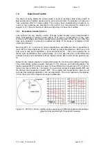
TVI XIIMUS cameras utilise a two channel CDD for each colour. A simplified illustration of the 
analogue video path of one channel is in figure 4.1. The video path itself is completely ana-
logue until digitised with 12-bit resolution in close vicinity of the CCD itself. All adjustments 
performed on the analogue video signal are digitally controlled. 
 

Figure 4.1.  

Analogue video path 

 
The analogue video signal is first Correlate Double Sampled and amplified in the preamp 
gain stage. After the CDS block it is possible to further amplify the signal with an analogue 
gain stage.  
 
The analogue video path also includes an input clamp circuit that is not drawn in the illustra-
tion. The input clamp circuit removes the CCD’s optical black offset to maximise system 
headroom and the effect of gain change on the black level. The effect of this circuit causes 
the digital output data to start from zero when the CCD is exposed to dark. If desired, the 
dark level register can be used to set a positive offset in the output data. If this parameter 
differs from zero, the dark level of channel in question will have an offset equal to the dark 
level setting. Changing this setting can be desirable when using the pixel correction unit, 
since the pixel to pixel variations in dark will be present in the raw data enabling better cor-
rection. 
 
Lastly the 12-bit data streams from the two output channels are digitally multiplexed into one 
data stream to represent the CCD output.  

© TVI Vision, 18 October 2006                                                                                                      page 11 ( 57 )   

Summary of Contents for 1024CTI

Page 1: ...hange any information in this document without prior notice TVI Vision Oy will not take any responsibility for any damage caused by possible inaccuracies or faults in the equipment This document may n...

Page 2: ...B User Manual 0 2 29 Mar 2006 jjl Updates until App B 1 0 2 June 2006 nr jjl First release 1 1 9 June 2006 nr Appendix C Serial communications Firmware updates D11 D13 and D12 D14 Read out of temperat...

Page 3: ...89 336 EEC EMC ELECTROMAGNETIC COMPATIBILITY WE HEREWITH DECLARE THAT THIS PRODUCT COMPLIES WITH THE FOLLOWING PROVISIONS APPLYING TO IT Emission CISPR 22 1997 Immunity IEC 61000 6 2 1999 APPLICABLE...

Page 4: ...RATIONS 21 7 1 SPECTRAL RESPONSE 21 7 2 SELECTION OF OPTICS 22 7 2 1 Modulation transfer function 22 7 2 2 Resolution and field of view 23 7 2 3 Depth of field and working aperture 24 8 LIGHTING 25 8...

Page 5: ...y and precise colour recognition The applications for the XIIMUS cameras include web inspection inspection of natural materials like food wood ore minerals and lumber recycling quality control in prin...

Page 6: ...accessed from the front If there are small amounts of contaminants or dust on the prism surface use a clean lint free cotton swab or other non abrasive medium dipped in acetone or pure alcohol to clea...

Page 7: ...ds above the require ments of CE conformity This may cause erroneous operation of the camera Transporting Preferably transport the camera in its original packaging If the package is discarded please p...

Page 8: ...and at the same time Corresponding pixels of all the three sensors are very precisely positioned optically in the same place figure 3 2 This makes the colour analysis simpler and does not require mat...

Page 9: ...amera responds by sending out the digital data stream of the previous line scan period time The output frequency is constant The distance in time between two NewLine edges can be set to any value abov...

Page 10: ...run mode both the line rate and the integration time can be precisely controlled But if the line rate is determined by encoder input the integration time can best be kept constant by using the encode...

Page 11: ...includes an input clamp circuit that is not drawn in the illustra tion The input clamp circuit removes the CCD s optical black offset to maximise system headroom and the effect of gain change on the...

Page 12: ...rIrIr RRR GbGbGb Ir Within a single colour pixel the data is ordered into a multiplier and an offset The multiplier consists of 14 bits and the offset of 10 bits Thus the three bytes that make up the...

Page 13: ...the original data is scaled up stretched to cover a larger range By altering the content of the shifter register it is possible to reset the multiplier unity level to any power of two between 128 and...

Page 14: ...depending on the unity mul tiplier level set in the shifter register Example The shifter register is set to 7 which equals 128 as a unity multiplier The digital gains are set to 7 as well which equals...

Page 15: ...t the beginning of the infrared line the lowest pixel value at level L2 has to be multiplied with a multiplier IRx so that it equals line L1 Accordingly at the start of the bluegreen channel line the...

Page 16: ...is a hardware method to move the port to RS 232 connector instruct tions available on request Six indicator LEDs on the right hand side show the status of the camera Figure 5 1 The rear panel layout...

Page 17: ...ded and the camera operation has been shut down After the external tem perature has fallen into the specified range switch the power once OFF and then ON again The camera did not start up properly Che...

Page 18: ...elay period is the line rate CC2 Exposure Control IR or all channels exposure control signal for the IR channel the effect for this is defined by the mode that is selected via RS 232 interface or Came...

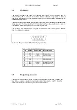
Page 19: ...ions Please specify the port when ordering cameras The connector is a standard 9 pin plug type connector with the following pin out as seen from the behind of the camera Figure 5 2 The pin numbers of...

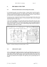
Page 20: ...ing holes at the side of the camera body First possibility is to fasten the camera with four screws to a special mounting stand The second option is to use a normal camera tripod using a standardised...

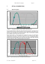
Page 21: ...ellent colour separation compared to trilinear CCD sensors Please note that this is an internal property of the camera and is shown only to describe the optical quality of the prism incl details of th...

Page 22: ...ons and diffraction this is impossible to reach MTF at large apertures f1 0 2 8 is limited by optical imperfections which vary a lot from lens to lens and manufacturer At small apertures f11 f32 lens...

Page 23: ...curacy by an image processing software Because of the CCD the fastest transition from black to white can occur within one pixel When using large apertures large field of view and the 2K sensor and dep...

Page 24: ...e central area of the lens is used The optical picture is more correct and resolution improves Considering this fact the lens to be used should have a large maximum aperture and should be operated at...

Page 25: ...iltered out or the source of lighting must be chosen so that the content of undesired wavelengths is minimised 8 2 Uniformity of lighting Uniformity of lighting means that there are negligible variati...

Page 26: ...fication to be done this aspect should be carefully considered The temperature dependency of the chosen light source should be verified For example fluorescent tubes have a relatively high relation be...

Page 27: ...max line rate 18 6 kHz Gain control G 100 x response time 500 ms max A D conversions 12 bit Supply voltage Vsupp 20 24 36 Vdc ripple 10 voltage ripple must stay within 20 to 36 V Power consumption 12...

Page 28: ...12 x 100 x response time 500 ms max A D conversions 12 bit Supply voltage Vsupp 20 24 36 Vdc ripple 10 voltage ripple must stay within 20 to 36 V Power consumption 12 17 26 W Weight m 1 3 kg without...

Page 29: ...ink output bit port assignments B Timing diagrams B1 Parallel colour channels output modes B2 Multiplexed colour cannels output modes C Serial communications D Model numbers E Ordering codes F Applica...

Page 30: ...GB 11 GB 0 4 GB 4 GB 2 GB 0 GB 2 GB 0 GB 1 5 GB 5 GB 3 GB 1 GB 3 GB 1 GB 2 6 GB 6 GB 4 GB 2 GB 4 GB 2 GB 3 7 GB 7 GB 5 GB 3 GB 5 GB 3 GB 4 8 GB 8 GB 6 GB 4 GB 6 GB 4 GB 5 9 GB 9 GB 7 GB 5 GB 7 GB 5 G...

Page 31: ...nit T1 NewLine low CC1 80 ns T2 Line Scan Period 3 x 512 pixels 20 MHz 25 MHz 33 3 MHz 40 MHz 3 x 1024 pixels 20 MHz 25 MHz 33 3 MHz 40 MHz 3 x 2048 pixels 20 MHz 25 MHz 33 3 MHz 40 MHz 30 1 24 2 18 3...

Page 32: ...Ti Multiplexed Output Modes Symbol Parameter Min Max Unit T1 NewLine low CC1 80 ns T2 Line Scan Period 3 x 512 pixels 8 3 MHz 16 7 MHz 3 x 1024 pixels 8 3 MHz 16 7 MHz 3 x 2048 pixels 8 3 MHz 16 7 MHz...

Page 33: ...included please contact TVI Vision for details and upgrades sales tvivision com This document describes the communication and all the available functions as low level details for developing users own...

Page 34: ...register command and the second byte is the data new value The camera responds to each valid setting by sending the same values back 8 bit address and 8 bit data Invalid commands are acknowledged with...

Page 35: ...ents of the selected memory bank or the current settings in use see corresponding sections for details In addition to the commands that modify registers there are several commands that retrieve inform...

Page 36: ...rt Loading and saving of correction data to or from the nonvolatile memory of the camera is also supported The written set of coefficients will be used for calculations performed by the Pixel Correcti...

Page 37: ...ng and the amount of bytes to be received The third operation will retrieve previously saved correction data from the nonvolatile memory to the camera for use The loaded set of coefficients will be th...

Page 38: ...l frequency per colour channel 3 3 2 Read Serial Number RS 232 port When this command is issued the ten byte serial number of the camera in question is output on the RS 232 port in ASCII text format T...

Page 39: ...V1 V0 Interpretation 0 0 1024 pixels 0 1 2048 pixels 1 0 4096 pixels 1 1 512 pixels Please contact TVI if this setting is not correct as it will affect correct operation of the camera The second data...

Page 40: ...data byte pairs See below in Memory functions for more details 3 5 Memory functions addresses 190 and 191 The internal nonvolatile memory of the camera is divided into 64 so called memory banks Each...

Page 41: ...t Communication ends when all 64 command and data byte pairs have been output and acknowledged on the serial port NOTE Data storage is guaranteed only up to 100 000 SAVE commands All the memory banks...

Page 42: ...l odd even decimal hexadecimal binary INFRARED odd 194 C2 1100 0010 even 195 C3 1100 0011 RED odd 198 C6 1100 0110 even 199 C7 1100 0111 BLUEGREEN odd 202 CA 1100 1010 even 203 CB 1100 1011 Example 1...

Page 43: ...inactive respective channel is never reset by the Exposure Control or to be always active pixels are reset all the time by the Exposure Control this results to a dark output value for the selected ch...

Page 44: ...s MSB first X X X X X D2 D1 D0 The last 3 bits are used for each colour channel see table below As default these are all zeros and there is no need to change them due to the sensitivity of the camera...

Page 45: ...default 1 Camera at slower output mode Bit SP is defined as Don t Care X for cameras which do not have two output modes Note The minimum STRB PixelStrobe frequency of the Camera Link standard is 20 M...

Page 46: ...The setting of this register defines which digital number is interpreted as multiplying with unity This register setting is meaningful only when correction is enabled Function decimal hexadecimal bin...

Page 47: ...by a full ramp in the next pixels The same applies to pairs of R1 and R0 as well as for Gb1 and Gb0 Bit AC selects the auto clocking mode 0 normal operation default 1 Auto clocking mode enabled In the...

Page 48: ...If this parameter is set the dark level of channel in question will have an offset equal to the dark level setting Function decimal hexadecimal binary Dark Level Infrared odd channel 217 D9 1101 1001...

Page 49: ...er is associated with the serial communications port The setting of this register defines which baud rate will be used for serial communication Both communications ports can be individually set to the...

Page 50: ...note that if the baud rate is changed the new setting must be saved to a memory bank using the new baud rate If the new baud rate is desired to be available at power up this new setting must be saved...

Page 51: ...ank for RGB channels 4 Pixel size of the sensors 14 for cameras with 14 m square sensors available for 512 1K and 2K pixel resolutions blank for all 10 m models 5 Read out rate of each colour channel...

Page 52: ...4 14 x 14 m not available with 4096 pixel sensors 5 Mode of the data interface P LVDS Parallel output 36 bits in parallel R G B or IR R GB sent out in parallel M1 LVDS Multiplexed output 12 bits in pa...

Page 53: ...configuration C12 Camera Link 36 bit RGB IR R GB for Medium configuration Note Each Camera Link camera contains either all the modes C5 to C10 or all the other modes The selection within each group is...

Page 54: ...t delay Use of encoder inputs for triggering the change of line Let us first define two terms 1 Line scan period is the time that the pixels are exposured to light This is the time between two rising...

Page 55: ...ossible inaccuracies in the frequency of the encoder input will affect only the duration of the T9 This delay has no meaning as long as the specified minimum duration is not violated Processing the co...

Page 56: ...w power low noise fan blowing air towards the internal hot spots of the camera Exhaust air flows out of the small holes near the rear plate All optical parts are protected against possible contaminati...

Page 57: ...to the camera 7 Press the latch on the fan side connector to open the connection 8 Replace the fan If the spare part was delivered by TVI Vision it is identical with the original part and has the conn...

Reviews: