KC724 GTX Transceiver Characterization Board
17
UG932 (v2.2) October 10, 2014
Detailed Description
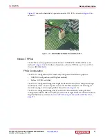
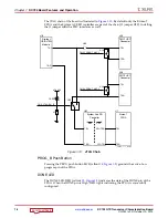
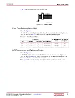
shows the heatsink fan power connector J121. J121 is shown in
as
callout
Kintex-7 FPGA
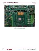
The KC724 board is populated with the Kintex-7 XC7K325T-3 FFG900E FPGA at U1
(callout
). For further information on Kintex-7 FPGAs, see
7 Series FPGAs
Overview
(DS180)
FPGA Configuration
The FPGA is configured in JTAG mode only using one of the following options:
•
USB JTAG configuration port (Digilent module)
•
System ACE SD controller
The FPGA is configured through the Digilent onboard USB-to-JTAG configuration logic
module (U8) where a host computer accesses the KC724 board JTAG chain through a
standard-A plug to micro-B plug USB cable. (callout
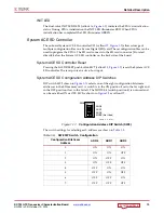
The FPGA is configured through the System ACE SD controller by setting the 4-bit
configuration address DIP switch (SW8) to select one of eight bitstreams stored on a Secure
Digital (SD) memory card (see
System ACE SD Configuration Address DIP Switches,
X-Ref Target - Figure 1-9
Figure 1-9:
Heatsink Fan Power Connector J121
UG9
3
2_c1_09_080612


