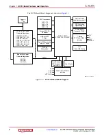
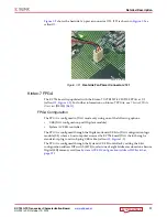
KC724 GTX Transceiver Characterization Board
19
UG932 (v2.2) October 10, 2014
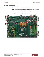
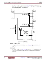
Detailed Description
INIT LED
The dual-color INIT LED DS25 (callout
,
) indicates the FPGA's initialization
status. During FPGA initialization the INIT LED illuminates RED. When FPGA
initialization has completed the LED illuminates GREEN.
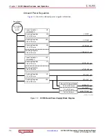
System ACE SD Controller
The onboard System ACE SD controller U32 (callout
,
) allows storage of
multiple configuration files on a Secure Digital (SD) card. These configuration files can be
used to program the FPGA. The SD card connects to the SD card connector J8 located
directly below the System ACE SD controller on the back side of the board.
System ACE SD Controller Reset
Pressing the SASD RESET push button SW7 (callout
) resets the System ACE
SD controller. The reset pin is an active-Low input.
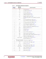
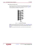
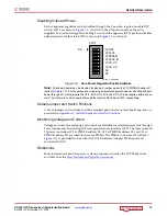
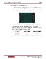
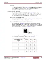
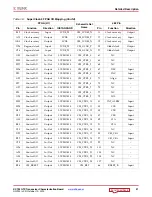
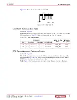
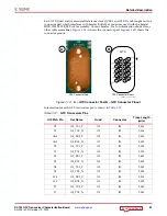
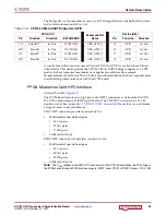
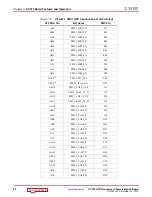
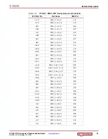
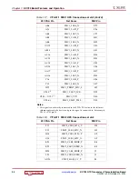
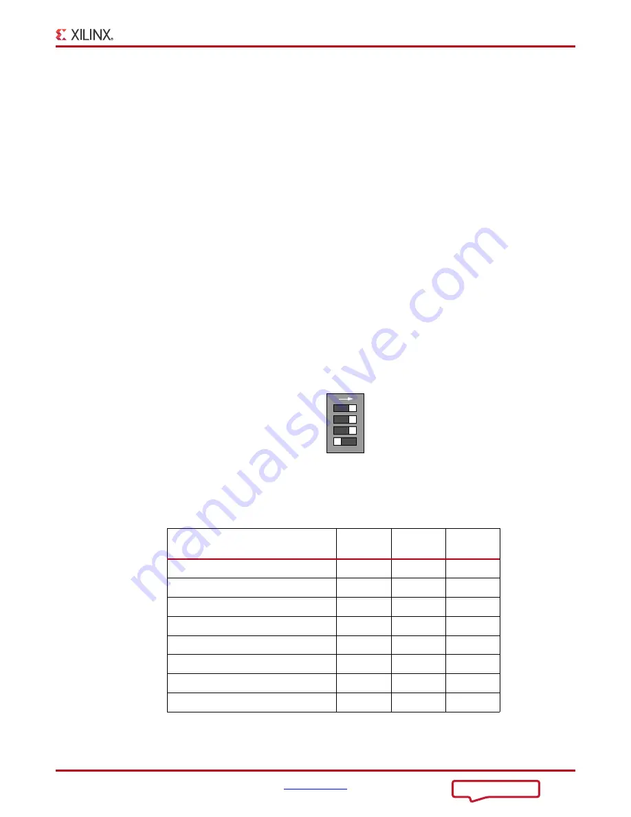
System ACE SD Configuration Address DIP Switches
DIP switch SW8 shown in
selects one of the eight configuration bitstream
addresses in the SD memory card. A switch is in the ON position if set to the far right and
in the OFF position if set to the far left. The MODE bit (switch position 4) is not used and
can be set either ON or OFF. SW8 is shown in
as callout
The switch settings for selecting each address are shown in
X-Ref Target - Figure 1-11
Figure 1-11:
Configuration Address DIP Switch (SW8)
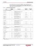
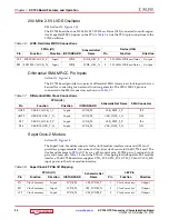
Table 1-5:
SW8 DIP Switch Configuration
Configuration Bitstream
Address
ADR2
ADR1
ADR0
0
ON
ON
ON
1
ON
ON
OFF
2
ON
OFF
ON
3
ON
OFF
OFF
4
OFF
ON
ON
5
OFF
ON
OFF
6
OFF
OFF
ON
7
OFF
OFF
OFF
UG932_c1_11_062712
ADR0
ADR1
ADR2
23
4
SW8
1
MODE (Not Used)
ON