8
KC724 GTX Transceiver Characterization Board
UG932 (v2.2) October 10, 2014
Chapter 1:
KC724 Board Features and Operation
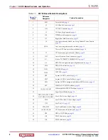
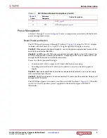
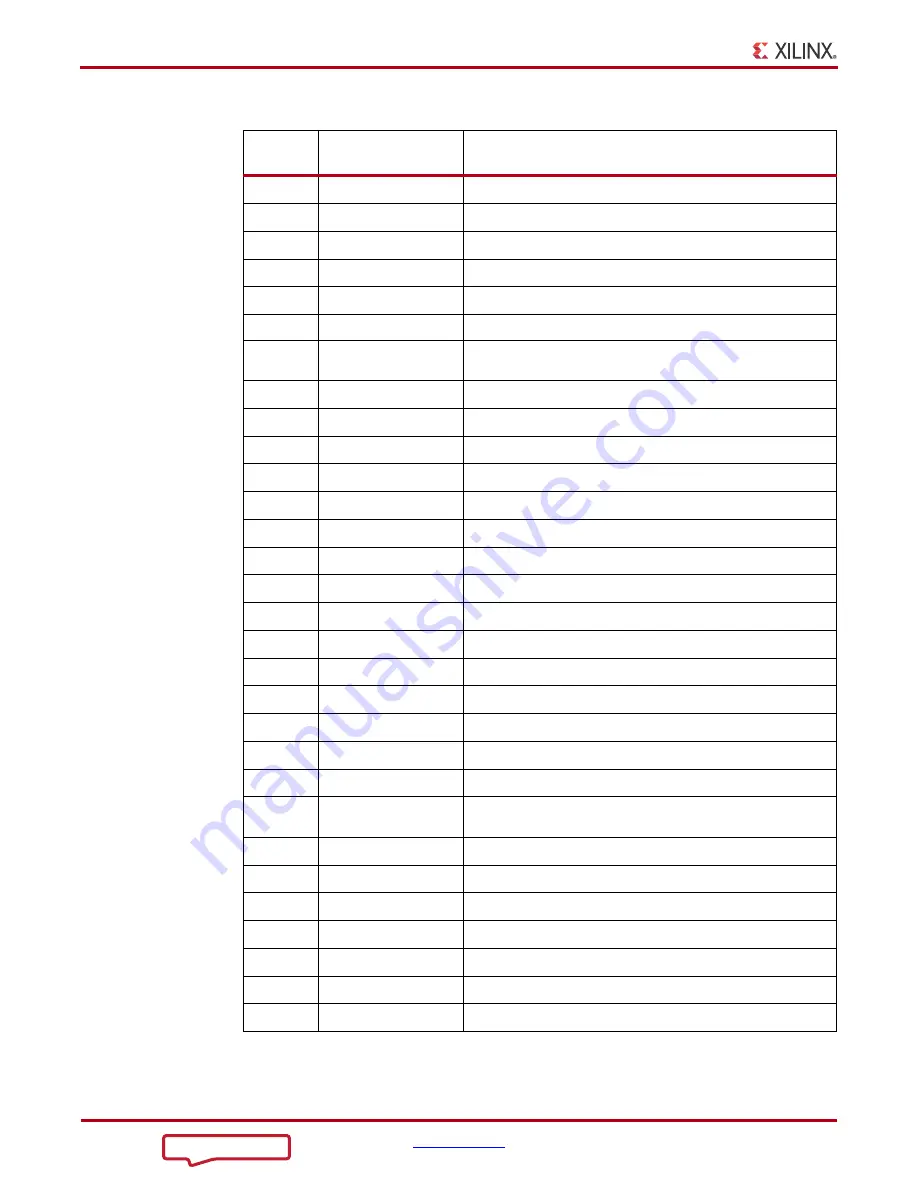
Table 1-1:
KC724 Board Feature Descriptions
Callout
Reference
Designator
Feature Description
1
SW1
Power Switch,
2
J2
12V Mini-Fit Connector,
3
J131
4
J5
12V Euro-Mag Connector,
5
J26
6
J27
Regulation inhibit connector,
7
J6
Core power terminal block (see Using External Power Sources,
8
SW10
Core power regulator enable switches,
9
7 Series GTX Transceiver Power Module,
10
J7
GTX transceiver power terminal block,
11
J121
Active Heatsink Power Connector,
12
U1
Kintex-7 XC7K325T-3 FFG900E FPGA,
13
U8
USB JTAG configuration port (Digilent module),
14
SW3
15
DS21
16
DS25
17
U32
18
SW7
System ACE SD Controller Reset,
19
SW8
System ACE SD Configuration Address DIP Switches,
20
U35
21
J98, J99, J100, J101
Differential SMA MRCC Pin Inputs,
22
23
DS13, DS14, DS15, DS16,
DS17, DS18, DS19, DS20
24
SW2
User DIP Switches (Active High),
25
J125
User Test I/O,
26
SW4, SW5
User Push Buttons (Active High),
27
J83, J84, J85, J86
GTX transceiver connector pads,
28
U34
29
JA2
30
JA3

