22
KC724 GTX Transceiver Characterization Board
UG932 (v2.2) October 10, 2014
Chapter 1:
KC724 Board Features and Operation
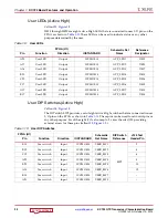
User LEDs (Active High)
Callout
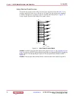
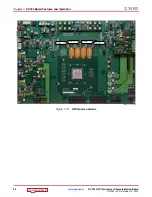
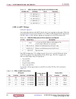
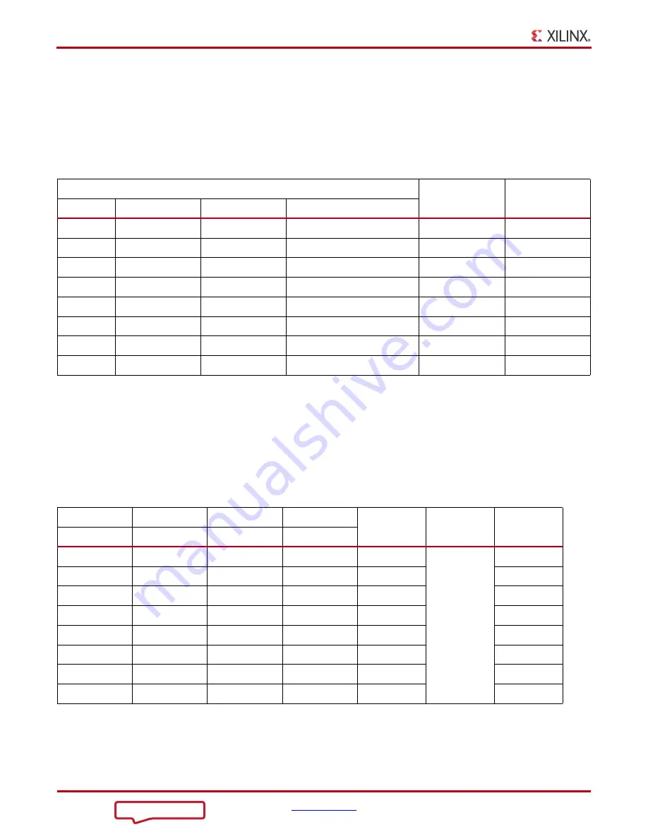
DS13 through DS20 are eight active-High LEDs that are connected to user I/O pins on the
FPGA as shown in
These LEDs can be used to indicate status or any other
purpose determined by the user.
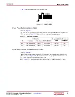
User DIP Switches (Active High)
Callout
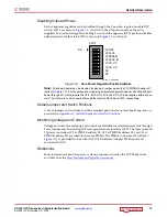
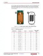
The DIP switch SW2 provides a set of eight active-High switches that are connected to user
I/O pins on the FPGA as shown in
. These pins can be used to set control pins or
any other purpose. Six of the eight I/Os also map to 2 x 6 test header J125 providing
external access for these pins (callout
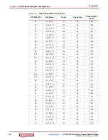
Table 1-9:
User LEDs
FPGA (U1)
Schematic Net
Name
Reference
Designator
Pin
Function
Direction
IOSTANDARD
A20
User LED
Output
LVCMOS18
APP_LED1
DS19
A17
User LED
Output
LVCMOS18
APP_LED2
DS20
A16
User LED
Output
LVCMOS18
APP_LED3
DS17
B20
User LED
Output
LVCMOS18
APP_LED4
DS18
C20
User LED
Output
LVCMOS18
APP_LED5
DS16
F17
User LED
Output
LVCMOS18
APP_LED6
DS15
G17
User LED
Output
LVCMOS18
APP_LED7
DS13
B17
User LED
Output
LVCMOS18
APP_LED8
DS14
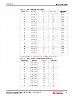
Table 1-10:
User DIP Switches
FPGA (U1)
Schematic
Net Name
DIP Switch
Reference
J125 Test
Header Pin
Pin
Function
Direction
IOSTANDARD
E18
User switch
Input
LVCMOS18
USER_SW1
SW2
2
B19
User switch
Input
LVCMOS18
USER_SW2
4
C19
User switch
Input
LVCMOS18
USER_SW3
6
A22
User switch
Input
LVCMOS18
USER_SW4
8
B22
User switch
Input
LVCMOS18
USER_SW5
10
A18
User switch
Input
LVCMOS18
USER_SW6
12
B18
User switch
Input
LVCMOS18
USER_SW7
–
A21
User switch
Input
LVCMOS18
USER_SW8
–

