KC724 GTX Transceiver Characterization Board
23
UG932 (v2.2) October 10, 2014
Detailed Description
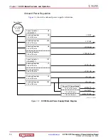
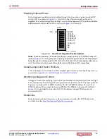
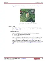
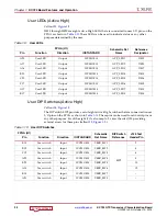
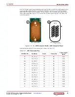
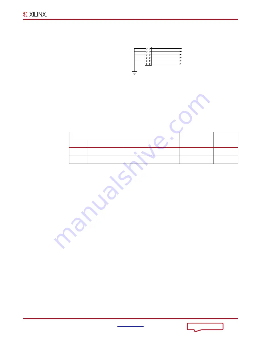
Shows the user test I/O connector J125.
User Push Buttons (Active High)
Callout
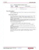
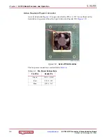
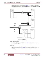
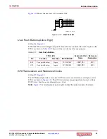
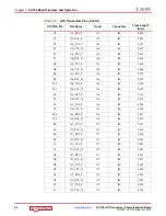
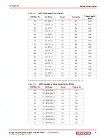
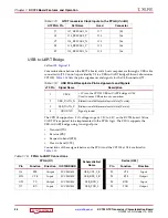
SW4 and SW5 are active-High user push buttons that are connected to user I/O pins on the
FPGA as shown in
. These switches can be used for any purpose.
GTX Transceivers and Reference Clocks
Callout
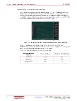
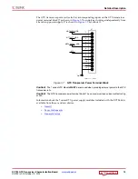
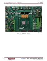
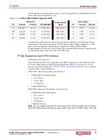
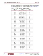
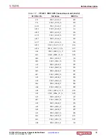
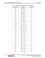
The KC724 board provides access to all GTX transceiver and reference clock pins on the
FPGA as shown in
. The GTX transceivers are grouped into four sets of four
RX-TX
lanes
. Four lanes are referred to as a
Quad
.
Note:
is for reference only and might not reflect the current revision of the board.
X-Ref Target - Figure 1-12
Figure 1-12:
User Test I/O
UG932_C1_12_062712
USER_SW1
9
8
7
6
5
4
3
2
10
1
12
11
J125
GND
USER_SW2
USER_SW3
USER_SW4
USER_SW5
USER_SW6
Table 1-11:
User Push Buttons
FPGA (U1)
Schematict Net
Name
Reference
Designator
Pin
Function
Direction
IOSTANDARD
K18
User push button
Input
LVCMOS18
USER_PB1
SW5
G19
User push button
Input
LVCMOS18
USER_PB2
SW4

