AXI Bridge for PCI Express v2.4
42
PG055 June 4, 2014
Chapter 3
Designing with the Core
This chapter includes guidelines and additional information to make designing with the
core easier.
General Design Guidelines
The Xilinx® Vivado® Design Suite has been optimized to provide a starting point for
designing with the AXI Bridge for PCI Express® core.
Clocking
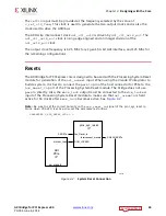
shows the clocking diagram for the core. The main memory mapped AXI4 bus
clock
axi_aclk
is driven by
axi_aclk_out
.
IMPORTANT:
axi_aclk_out
and
axi_ctl_aclk_out
are connected to
axi_aclk
and
axi_ctl_aclk
, respectively, and they do not need to be connected in the design.
X-Ref Target - Figure 3-1
Figure 3-1:
Clocking Diagram
!8)
0#)E
)0
AXI?ACLK
AXI?CTL?ACLK
AXI?ACLK?OUT
AXI?CTL?ACLK?OUT
MMCM?LOCK
REFCLK
0#)E2EFERENCE#LOCK


