background image

12

www.xilinx.com

ML501 Getting Started Tutorial

UG228 (v1.0) August 30, 2006

ML501 Demonstrations in System ACE CF

R

ML501 Demonstrations in System ACE CF

Bootloader Demonstrations

To select configuration using System ACE CF, set the configuration address and mode DIP 
switch (8-position DIP switch) to 

00010101

. To return to the ML501 Bootloader at 

anytime, press the SYSACE RESET button. 

Location

System ACE configuration address 0.

Description

The ML501 Bootloader demonstration displays a menu of demonstration designs that can 
be loaded by using the System ACE controller’s reconfiguration feature. The menu is 
displayed on the serial terminal, LCD, and VGA.

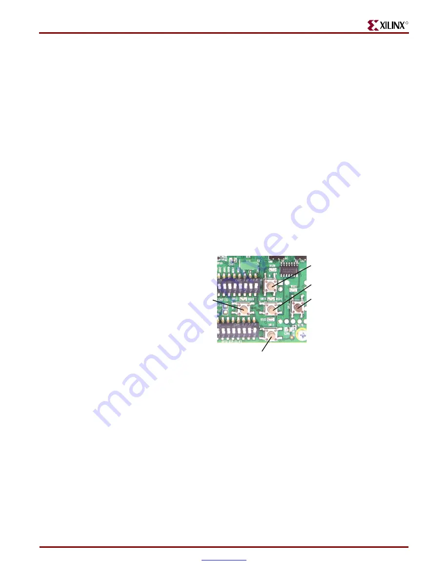
To choose a demonstration, use the North-East-South-West-Center-oriented pushbuttons 
on the board (

Figure 5

), then press the center button to start the demonstration. 

Alternatively, you can select a demonstration by entering its number into the serial 
terminal. 

The demonstrations are:

“Virtex-5 Slide Show,” page 13

“Web Server (Using Soft Ethernet MAC),” page 14

“Simon Game,” page 16

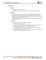
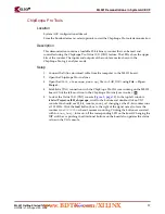
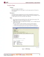
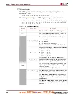
“ChipScope Pro Tools,” page 17

“USB,” page 19

“My Own ACE File,” page 20

“Ring Tone Player,” page 21

Figure 5:

User Pushbuttons

UG0

83

_05_0

83

006

We

s

t (W)

S

o

u

th (

S

)

E

as

t (E)

North (N)

Center (C)

www.BDTIC.com/XILINX

Summary of Contents for ML501

Page 1: ...R ML501 Getting Started Tutorial For ML501 Evaluation Platforms UG228 v1 0 August 30 2006 www BDTIC com XILINX...

Page 2: ...ITS AGENTS OR EMPLOYEES XILINX MAKES NO OTHER WARRANTIES WHETHER EXPRESS IMPLIED OR STATUTORY REGARDING THE DESIGN INCLUDING ANY WARRANTIES OF MERCHANTABILITY FITNESS FOR A PARTICULAR PURPOSE TITLE AN...

Page 3: ...cation 14 Description 14 Setup 14 Simon Game 16 Location 16 Description 16 Instructions 16 ChipScope Pro Tools 17 Location 17 Description 17 Setup 17 USB 19 Location 19 Description 19 Setup 19 My Own...

Page 4: ...up 24 Platform Flash XROM Demonstration 24 Location 24 Description 24 Setup 24 My Own Platform Flash Image Demonstration 25 Description 25 ML501 Demonstrations in SPI Flash 26 SPI Flash Hello Demonstr...

Page 5: ...tains the DC and Switching Characteristic specifications for the Virtex 5 family XtremeDSP Design Considerations This guide describes the XtremeDSP slice and includes reference designs for using the D...

Page 6: ...e Virtex 5 Configuration Guide for more information Emphasis in text The address F is asserted after clock event 2 Underlined Text Indicates a link to a web page http www xilinx com virtex5 Convention...

Page 7: ...tions use a computer installed with Xilinx ISE 8 2i Service Pack 2 Xilinx Platform Studio 8 2i Service Pack 1 ChipScope Pro 8 2i Service Pack 2 The following additional equipment is also recommended D...

Page 8: ...om the board Figure 1 shows the back side of the board with the CF card properly inserted Note The CF card provided with your board might differ Caution Be careful when inserting or removing the CF ca...

Page 9: ...ect Start Programs Accessories Communications HyperTerminal In the Connection Description window type 9600 in the Name box then click OK In the Connect To window click Cancel In the 9600 HyperTerminal...

Page 10: ...et the COM1 properties Figure 3 to the following Bits per second 9600 Data bits 8 Parity None Stop bits 1 Flow control None Click OK OK to accept settings 7 Select File Properties 8 Select the Setting...

Page 11: ...been programmed the LEDs in the lower left corner should be Bus Error 1 and 2 off FPGA INIT green FPGA DONE green System ACE Err off System ACE Stat green Note When the CF card is ejected or not inst...

Page 12: ...designs that can be loaded by using the System ACE controller s reconfiguration feature The menu is displayed on the serial terminal LCD and VGA To choose a demonstration use the North East South Wes...

Page 13: ...reConnect bus Setup To change or customize the side show follow these instructions 1 Place the picture files in the root directory 2 Name the picture files image XX bmp where XX is a numerical sequenc...

Page 14: ...he current DIP switch values to be re read By default the IP address of the ML501 board is 1 2 3 4 but it can be changed by recompiling the software Setup 1 Connect an Ethernet cable straight or cross...

Page 15: ...stablished at that speed You might need to force your computer to link in 10 or 100 Mb s duplex mode If so then Right click Local Area Connection Properties Configure Advanced tab Speed 4 On the remot...

Page 16: ...d on the character LCD and on the video screen Note Note This demonstration requires a DVI monitor or a VGA monitor with DVI to VGA adapter connected to the DVI port Instructions At the beginning of t...

Page 17: ...pe Pro Analyzer 3 Open the ML501_chipscope_demo cpj file in LAB_DIR using File Open Project 4 Establish a JTAG connection with the ChipScope Pro ILA core running on the ML501 board Click the left most...

Page 18: ...rations in System ACE CF R 6 Look at the waveform window Select Window Waveform DEV 3 My ILA 7 Click the trigger immediate T button 8 Use the magnifying glass icon to zoom in to see the individual 32...

Page 19: ...re for the internal microprocessor inside the USB controller Cypress CY7C76300 The FPGA s processor reads this file and writes the data to the memory inside the USB controller through its HPI port The...

Page 20: ...This creates the my_button_led_test_hw ace file 4 Carefully remove the System ACE CF card from the ML501 board preferably with the power off Open the CF card on your computer This requires either a PC...

Page 21: ...a serial terminal program users can play ring tones from a CF card or type in their ring tones Setup 1 The start screen ask you to insert the CF card which contains the ring tones in the ringtone fold...

Page 22: ...te as follows 1 is a whole note 2 is a half note 4 is a quarter note and so forth If the duration is not specified the default is d 4 o 4 5 6 7 Parameter o specifies the octave of a note Note a for ea...

Page 23: ...ogram it onto the FPGA This exercise overwrites the contents of linear flash To program your own bit file into linear flash 1 Open a DOS command shell Click Start Menu Run then enter cmd as the progra...

Page 24: ...Platform Flash LCD Demonstration Location Platform Flash configuration address 0 Description This demonstration displays to the character LCD the message Put Your Design Here Setup 1 Set the configur...

Page 25: ...ype cd LAB_DIR 4 Copy your bit file into this folder Copy file_name bit 5 Format the BIT file to an MCS file Type in the command prompt promgen w p mcs o file_name mcs s 16384 u 0 file_name bit 6 Now...

Page 26: ...device that can store your configuration file and program it to the FPGA This demonstration shows you how to store your own design into the SPI Flash and how to program it onto the FPGA This exercise...

Page 27: ...iguration tab and select Add SPI Device 11 Navigate to file_name mcs created above and click Open 12 In the Select Device Part Name drop down dialog box select M25P16 and click OK 13 The Direct SPI Co...

Page 28: ...28 www xilinx com ML501 Getting Started Tutorial UG228 v1 0 August 30 2006 ML501 Demonstrations in SPI Flash R www BDTIC com XILINX...

Reviews: