background image

ML505/ML506/ML507 Getting Started Tutorial

www.xilinx.com

13

UG348 (v3.0.2) October 9, 2008

Board Setup

R

9.

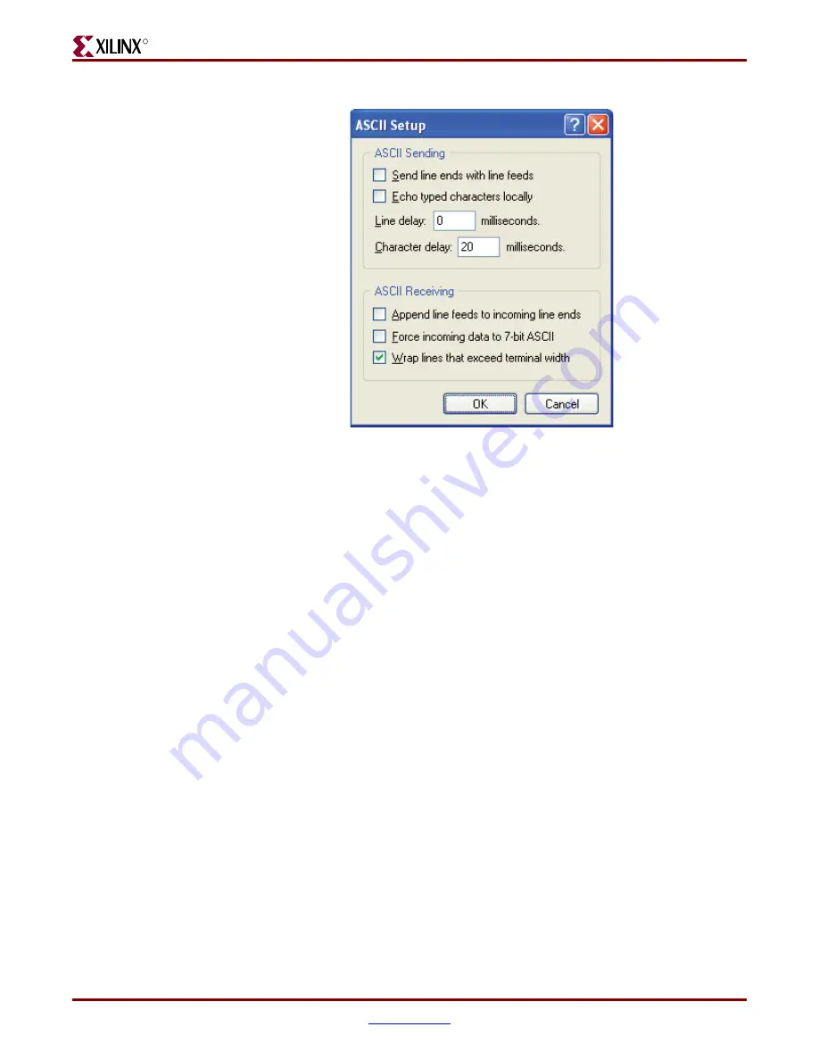
For Character delay, enter 20.

10. Click 

OK


OK 

to accept the settings.

11. Connect the DVI monitor or the VGA monitor with DVI-to-VGA adapter to the board, 

if available.

12. Turn on the ML50

x

 board’s main power switch and press the SYSACE RESET button. 

After the FPGA has been programmed, the LEDs in the lower left corner should be:

Bus Error 1 and 2 = off

FPGA INIT = green

FPGA DONE = green

System ACE “Err” = off

System ACE “Stat” = green

Note:

When the CF card is ejected or not installed, the System ACE “Err” LED blinks. 

13. Extract the associated training lab files to your local computer. 

[Ref 3]

Unzip the training lab files to a working directory, name the directory, and make note 
of the directory’s name. This directory with the extracted files is referred to as 
<

LAB_DIR

> in this tutorial.

Figure 5:

ASCII Setup

UG

3

4

8

_05_04040

8

www.BDTIC.com/XILINX

Summary of Contents for ML505

Page 1: ...R ML505 ML506 ML507 Getting Started Tutorial For ML505 ML506 ML507 Evaluation Platforms UG348 v3 0 2 October 9 2008 PN 0402745 01 www BDTIC com XILINX...

Page 2: ...O OTHER WARRANTIES WHETHER EXPRESS IMPLIED OR STATUTORY REGARDING THE DOCUMENTATION INCLUDING ANY WARRANTIES OF MERCHANTABILITY FITNESS FOR A PARTICULAR PURPOSE OR NONINFRINGEMENT OF THIRD PARTY RIGHT...

Page 3: ...scription 14 Virtex 5 FPGA Slide Show 15 Location 15 Description 15 Setup 15 Web Server ML505 ML506 Using Soft Ethernet MAC IP Core 16 Location 16 Description 16 Setup 16 Web Server ML507 Using Integr...

Page 4: ...on 26 Description 26 ML50x Demonstrations in Platform Flash 28 Platform Flash LCD Demonstration 28 Location 28 Description 28 Setup 28 Platform Flash XROM Demonstration 28 Location 28 Description 28 S...

Page 5: ...utlined in this overview Virtex 5 FPGA Data Sheet DC and Switching Characteristics This data sheet contains the DC and Switching Characteristic specifications for the Virtex 5 family Virtex 5 FPGA Use...

Page 6: ...mpassing configuration guide includes chapters on configuration interfaces serial and SelectMAP bitstream encryption Boundary Scan and JTAG configuration reconfiguration techniques and readback throug...

Page 7: ...See the Virtex 5 FPGA Configuration Guide for more information Emphasis in text The address F is asserted after clock event 2 Underlined Text Indicates a link to a web page http www xilinx com virtex5...

Page 8: ...8 www xilinx com ML505 ML506 ML507 Getting Started Tutorial UG348 v3 0 2 October 9 2008 Preface About This Guide R www BDTIC com XILINX...

Page 9: ...l Cable III IV or Platform Cable USB with JTAG flying wires adapter Additional information and support material is located at ML505 http www xilinx com ml505 ML506 http www xilinx com ml506 ML507 http...

Page 10: ...osition 3 Locate the CF card slot on the back side of the ML50x board and carefully insert the System ACE CF card with its front label facing away from the board Figure 1 shows the back side of the bo...

Page 11: ...S 2 connectors 6 Connect a null modem serial cable between your computer and the ML50x board and open a serial terminal program Select Start Programs Accessories Communications HyperTerminal In the Co...

Page 12: ...nu to set the COM1 properties Figure 4 to the following Bits per second 9600 Data bits 8 Parity None Stop bits 1 Flow control None Click OK OK to accept settings 7 Select File Properties 8 Select the...

Page 13: ...has been programmed the LEDs in the lower left corner should be Bus Error 1 and 2 off FPGA INIT green FPGA DONE green System ACE Err off System ACE Stat green Note When the CF card is ejected or not...

Page 14: ...em ACE controller s reconfiguration feature The menu is displayed on the serial terminal LCD and VGA To choose a demonstration use the North East South West Center oriented pushbuttons on the board Fi...

Page 15: ...internal CoreConnect bus Setup To change or customize the side show follow these instructions 1 Place the picture files in the root directory 2 Name the picture files image XX bmp where XX is a numer...

Page 16: ...e and the current DIP switch values to be re read By default the IP address of the ML505 and ML506 boards is 1 2 3 4 but it can be changed by recompiling the software Setup 1 Connect an Ethernet cable...

Page 17: ...is established at that speed You might need to force your computer to link in 10 or 100 Mb s duplex mode If so then Right click Local Area Connection Properties Configure Advanced tab Speed 4 On the r...

Page 18: ...nge and the current DIP switch values to be re read By default the IP address of the ML507 board is 192 168 1 10 but it can be changed by recompiling the software Setup 1 Connect an Ethernet cable str...

Page 19: ...established at that speed You might need to force your computer to link in 10 Mb s 100 Mb s or 1000 Mb s duplex mode If so then Right click Local Area Connection Properties Configure Advanced tab Spe...

Page 20: ...isplayed on the character LCD and on the video screen Note Note This demonstration requires a DVI monitor or a VGA monitor with DVI to VGA adapter connected to the DVI port Instructions At the beginni...

Page 21: ...oard diagnostics and testing Instructions On the terminal window associated with the serial port enter the number 1 to select the Tests sub menu Make further selections as desired to run board diagnos...

Page 22: ...software for the internal microprocessor inside the USB controller Cypress CY7C76300 The FPGA s processor reads this file and writes the data to the memory inside the USB controller through its HPI p...

Page 23: ...nerator GenACE chapter in the Embedded System Tools Reference Manual contains details on how to create ACE files Ref 16 4 Carefully remove the System ACE CF card from the ML50x board preferably with t...

Page 24: ...rough a serial terminal program users can play ring tones from a CF card or type in their ring tones Setup 1 The start screen ask you to insert the CF card which contains the ring tones in the rington...

Page 25: ...each note as follows 1 is a whole note 2 is a half note 4 is a quarter note and so forth If the duration is not specified the default is d 4 o 4 5 6 7 Parameter o specifies the octave of a note Note a...

Page 26: ...shows you how to store your own design into linear flash and how to program it onto the FPGA using the Embedded Development Kit EDK GUI A bitstream with a flash memory interface is provided in the ml...

Page 27: ...ss to 0x00000000 For Configuration 1 set the address to 0x00800000 For Configuration 2 set the address to 0x01000000 For Configuration 3 set the address to 0x01800000 Set the Scratch Memory Properties...

Page 28: ...506 Platform Flash configuration address 0 ML507 Platform Flash configuration address 1 Description This demonstration displays to the character LCD the message Put Your Design Here Setup 1 Set the co...

Page 29: ...pe cd LAB_DIR 4 Copy your bit file into this folder Copy file_name bit 5 Format the BIT file to an MCS file For an ML505 or ML506 board on one line type in the command prompt promgen w p mcs c FF o ml...

Page 30: ...re your own design into the SPI Flash and how to program it onto the FPGA This exercise overwrites the contents of the SPI Flash 1 Disconnect the cable attached to header J1 the header on the left sid...

Page 31: ...rces ML505 ML506 ML507 Documents supporting Virtex 5 FPGAs 4 DS100 Virtex 5 Family Overview 5 DS202 Virtex 5 FPGA Data Sheet DC and Switching Characteristics 6 UG190 Virtex 5 FPGA User Guide 7 UG200 E...

Reviews: