Hardware User Guide
3-14
Xilinx Development System
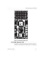
XC4003E Probe Points
All pins of the XC4003E connect to the headers that surround the
FPGA socket. These pins provide convenient points for probing
signals or making wirewrap connections to other circuitry, including
the prototype area. Pin numbering increases from the inside row to
the outside, counterclockwise. See the corners of each header for the
starting number of that header.
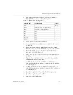
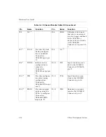
XC4003E Configuration Switches (SW2)
The following sections describe each of the SW2 switches. For more
information on configuring the XC40003E device, see the
PWR-Power (SW2–1)
This switch turns the unregulated power input on or off to the +5 V
regulator U3.
MPE-Multiple Program Enable (SW2-2)
With MPE turned on and SPE turned off, the configuration PROM
(U2) is reset by the RESET pushbutton (SW4). Configuration mode
must be set to master-serial. After a Reset or powerup, the first
bitstream stored in the serial PROM is loaded into the XC4003E.
Pressing RESET resets the serial PROM address pointer. Pressing
PROG (SW6) loads the XC4003E with the first bitstream again. If you
press PROG without pressing RESET, the XC4003E is loaded with the
next bitstream that is stored in the serial PROM. The size of the serial
PROM limits the number of bitstreams that can be sequentially
loaded.
SPE-Single Program Enable (SW2-3)
With SPE turned on and MPE turned off, the configuration PROM
(U2) is reset by the XC4003E’s INIT output, which is driven Low
whenever you press PROG (SW6). The first bitstream stored in the
serial PROM is loaded into the XC4003E.
Note
MPE and SPE must not be on at the same time, one must be off
when the other is on. MPE and SPE are only used in conjunction with


