FPGA Design Demonstration Board
Hardware User Guide
3-33
with power off. Use the appropriate demonstration board socket
for your device.
♦
U2 socket: XC4003E devices
♦
U2 socket: XC4003E and XC3020A devices in a daisy chain
with the XC4003E at the head of the chain
♦
U1 socket: XC3020A devices
5.
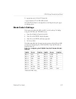
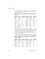
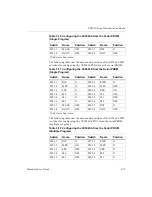
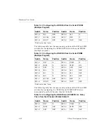
Set the mode switches.
When you use the serial PROMs, the M0, M1, and M2 switches
must be off. This setting causes the device to be in the active
master serial mode. Set the MPE, SPE, and RST switches to the
desired positions. Refer to the
and the
for
switch settings required to configure a daisy chain.
6.
Load the FPGA.
7.
After you insert the PROM into the socket and set the configura-
tion switches, apply power to the FPGA Demonstration Board.
This step configures the FPGA; when the DONE pin goes High, it
indicates that the design logic is active.
8.
Start your configuration software.
For information on starting the Hardware Debugger software, see the
following section.
Starting Hardware Debugger
The following section includes a checklist for opening the Hardware
Debugger software. For further information, consult the Hardware
Debugger Guide.
1.
Open your Alliance or Foundation software.
2.
From within Xilinx Design Manager (version M1.0 or later), select
Hardware Debugger from the tools menu. You can also start the
Hardware Debugger from the operating system prompt by
entering the following command.
hwdebugr design_name
When you start the Hardware Debugger, the port where the cable
is plugged in is located, and the baud rate is set to the maximum
allowed by the platform.


