FPGA Design Demonstration Board
Hardware User Guide
3-15
the serial PROMs. The serial PROMs must be configured as OE/Reset
to allow MPE and SPE to function properly.
M0, M1, M2-Mode Pins (SW2-4,5,6)
These three switches must be on to configure the XC4003E using the
XChecker/Parallel Cable III. When these switches are on, the FPGA is
in slave serial mode. To configure the XC4003E from the onboard
serial PROM, these three switches must be off. This places the FPGA
in master serial mode.
RST-Reset (SW2-7)
When this switch is on, it connects the RESET pushbutton (SW4) to
XC4003E pin 56.
INIT-Initialize (SW2-8)
When this switch is on, it connects the XC3020A INIT pin to the
XC4003E INIT pin. This connection is used to configure FPGAs in a
daisy chain with the XC4003E at the head of the chain.
Note
INIT should only be used to configure FPGAs in a daisy chain.
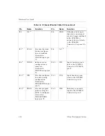
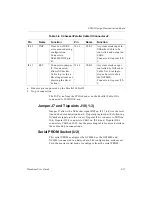
XChecker/Parallel Cable III Connector J2
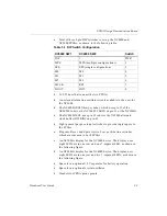
The following table provides a detailed description of the J2
XChecker/Parallel Cable III connector.
Table 3-6 XChecker/Parallel Cable III Connector J2
Pin
Name
Function
Pin
Name
Function
J2-1
a
VCC
Su5 V to the
cable.
J2-2
RT
Read Trigger allows
XChecker Cable to
trigger a readback of the
XC4003E.
Connects to XC4003E
pin 32.
J2-3
GND
Supplies ground
reference to the
cable.
J2-4
RD
Used by XChecker Cable
for readback data.
Connects to XC4003E
pin 30.


