background image

10

SP305 Spartan-3 Development Platform User Guide

www.xilinx.com

UG216 (v1.1) March 3, 2006


SP305 Spartan-3 Development Platform User Guide

R

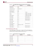
User LEDs (7)

There are 4 green LEDs are general purpose LEDs arranged in a row. The LEDs are active 
high LEDs directly controllable by the FPGA:

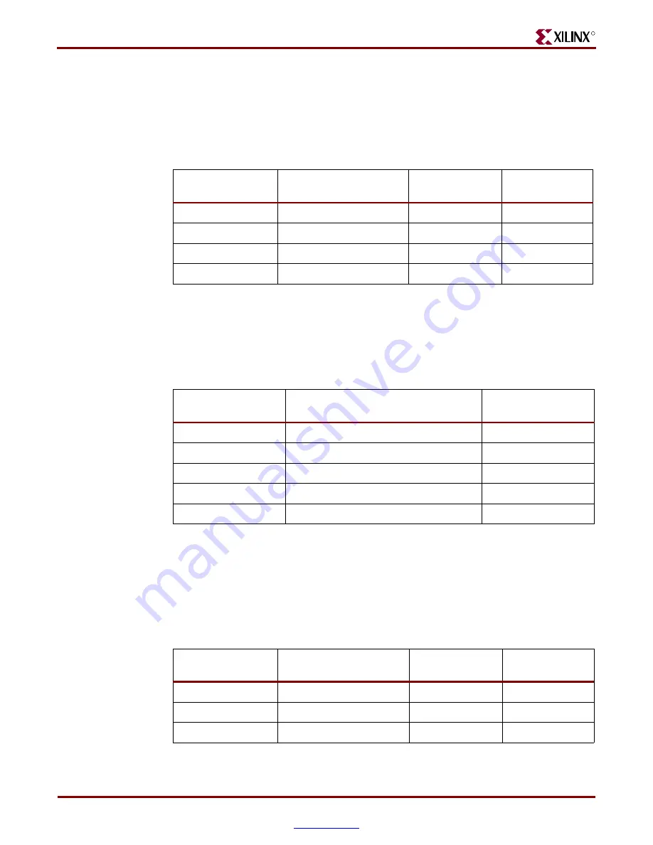
Table 2-4

 summarizes the LED definitions and connections

Reference

Designator

Label/Definition

Color

FPGA Pin

GPIO LED 0

GPIO LED 1

GPIO LED 2

GPIO LED 3

.

User Push Buttons (

8

)

There are five active-high user push buttons available for general purpose usage and are 
arranged in a


North-East-South-West-Center

 orientation (only the 

West

 one is cited in 

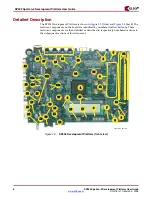
Figure 2-2, page 6

). The user push button connections are summarized in 

Table 2-5

.

Reference

Designator

Label/Definition

FPGA Pin

GPIO Switch North

GPIO Switch South

GPIO Switch East

GPIO Switch West

GPIO Switch Center

User Push Button LEDs (9)

There are 5 green LEDs positioned next to the 

North-East-South-West-Center

 oriented 

push buttons (only the 

Center

 one is called out in 

Figure 2-2, page 6

). The LEDs are active 

high and are directly controllable by the FPGA:

Table 2-6

 summarizes the LED definitions and connections.

Table 2-4: 

User LED Connections 

DS15

Green

J3

DS4

Green

J4

DS5

Green

D22

DS6

Green

E22

Table 2-5: 

User Push Button Connections 

SW3

H6

SW4

F3

SW5

G6

SW7

G4

SW6

F1

Table 2-6: 

User LED Connections 

Reference

Designator

Label/Definition

Color

FPGA Pin

DS14

LED North

Green

K6

DS3

LED South

Green

G5

DS11

LED East

Green

F4

Summary of Contents for SP305 Spartan-3

Page 1: ...UG216 v1 1 March 3 2006 SP305 Spartan 3 Development Platform User Guide www xilinx com SP305 Spartan 3 Development Platform User Guide UG216 v1 1 March 3 2006 ...

Page 2: ... AND AGREE THAT YOU HAVE NOT RELIED ON ANY ORAL OR WRITTEN INFORMATION OR ADVICE WHETHER GIVEN BY XILINX OR ITS AGENTS OR EMPLOYEES XILINX MAKES NO OTHER WARRANTIES WHETHER EXPRESS IMPLIED OR STATUTORY REGARDING THE DESIGN INCLUDING ANY WARRANTIES OF MERCHANTABILITY FITNESS FOR A PARTICULAR PURPOSE TITLE AND NONINFRINGEMENT OF THIRD PARTY RIGHTS IN NO EVENT WILL XILINX BE LIABLE FOR ANY CONSEQUENT...

Page 3: ...5 Spartan 3 Development Platform User Guide UG216 v1 1 March 3 2006 The following table shows the revision history for this document Version Revision 11 23 05 1 0 Initial Xilinx release 3 3 06 1 1 In USB Controller with Host and Peripheral Ports 25 section added note indicating non support for 2nd USB feature ...

Page 4: ...SP305 Spartan 3 Development Platform User Guide UG216 v1 1 March 3 2006 www xilinx com ...

Page 5: ... Buttons 8 10 User Push Button LEDs 9 10 CPU Reset Button 10 11 Program Switch 11 11 JTAG Configuration Port 12 11 Configuration Address and Mode DIP Switches 13 12 FPGA HSWAP_EN 14 12 Platform Flash Memory 15 13 Platform Flash Configuration Select 16 13 Platform Flash Enable and Reset Control 17 13 Done and INIT LED 18 13 Error LEDs Active High 19 13 RS 232 Serial Port 1 20 14 RS 232 Serial Port ...

Page 6: ... 2 Mouse and Keyboard Ports 33 27 ChipScope 34 27 CAN Controller MCP2515 and MPC2551 35 27 DDR SDRAM 36 29 ZBT Synchronous SRAM 37 29 Linear Flash Memory Chips 38 32 Expansion JTAG Jumper 39 34 Bank 3 Voltage selection 40 35 IIC Bus with 4Kb EEPROM 41 35 IFF 42 35 Default Jumper Settings 36 ...

Page 7: ...inx website at http www xilinx com literature index htm To search the Answer Database of silicon software and IP questions and answers or to create a technical support WebCase see the Xilinx website at http www xilinx com support Conventions This document uses the following conventions An example illustrates each convention Typographical The following typographical conventions are used in this doc...

Page 8: ...not connected Square brackets An optional entry or parameter However in bus specifications such as bus 7 0 they are required ngdbuild option_name design_name Braces A list of items from which you must choose one or more lowpwr on off Vertical bar Separates items in a list of choices lowpwr on off Vertical ellipsis Repetitive material that has been omitted IOB 1 Name QOUT IOB 2 Name CLKIN Horizonta...

Page 9: ...a push button shaft Expansion header with 32 single ended I O 16 LVDS capable differential pairs 14 spare I O s power JTAG chain expansion capability and IIC bus expansion Stereo AC97 audio codec with line in line out 50 mW headphone and microphone in mono jacks Two RS 232 serial port one stand alone and one attached to the USB Chipset 16 character x 2 line LCD display 4Kb IIC EEPROM VGA output wi...

Page 10: ...ion about the SP305 Development Platform including Current version of this user guide in PDF format Example design files for demonstration of Spartan 3 features and technology Demonstration hardware and software configuration files for the Platform Flash configuration storage device and linear flash memory chips MicroBlaze EDK reference design files Full schematics in PDF format and ViewDraw schem...

Page 11: ... FPGA I O Expansion Header IIC EEPROM 5V Brick 3A Platform Flash Flash Flash SEL MAP SLV SERIAL JTAG MSTR SERIAL 16 x 32 Character LCD Can Controller SPI AC97 Audio CODEC Line Out Headphone Video Mic In Line in RS 232 XCVR VGA Host Peripheral Peripheral Serial 10 100 1000 Enet Phy 10 100 Enet Phy DDR SDRAM DDR SDRAM 32 16 RJ 45 PC RJ 45 User IIC Bus JTAG JTAG 32 5V to USB and PS 2 TPS54310 3A SWIF...

Page 12: ...n the board are identified by numbered yellow balloons These features components are then detailed or described in respectively numbered sections in the subsequent sections of this document Figure 2 2 SP305 Development Platform front view 14 14 30 30 32 32 23 23 26 26 19 19 18 18 22 22 34 34 37 37 10 10 11 11 12 12 13 13 17 17 15 15 16 16 36 36 24 24 29 29 28 28 27 27 20 20 21 21 25 25 33 33 5 1 9...

Page 13: ...e other features components are numbered accordingly in the subsequent sections Configuration The board supports configuration in all modes JTAG Master Serial Slave Serial Master SelectMAP and Slave SelectMAP modes See the Configuration Options page 11 section for more information Figure 2 3 SP305 Development Platform back view 2 30 30 21 21 39 39 40 40 33 33 36 36 33 33 41 41 29 29 20 20 26 26 25...

Page 14: ... 10 or better than 10 The power switch turns the board on and off by controlling the supply of 5V to the board Power Indicator LED 3 The PWR Good LED lights when the 1 2V 2 5V and 3 3V power supplies are all at their nominal operating conditions If the PWR Good LED is off blinking or glowing lightly a fault condition such as a short or overload condition may exist On board Power Supplies 4 Power s...

Page 15: ...oscillator sockets accept half sized oscillators and are powered by the 3 3V supply Label Clock Name FPGA Pin SYSCLK USERCLK DIP Switches 6 There are eight general purpose active high DIP switches connected to the user I O pins of the FPGA See Table 2 3 for a summary of these connections SW1 FPGA Pin SW1 FPGA Pin Figure 2 4 Power Supply Diagram TPS54310 3A SWIFT TPS54310 6A SWIFT TPS51100 3A DDR L...

Page 16: ...n Figure 2 2 page 6 The user push button connections are summarized in Table 2 5 Reference Designator Label Definition FPGA Pin GPIO Switch North GPIO Switch South GPIO Switch East GPIO Switch West GPIO Switch Center User Push Button LEDs 9 There are 5 green LEDs positioned next to the North East South West Center oriented push buttons only the Center one is called out in Figure 2 2 page 6 The LED...

Page 17: ...allows for device programming and FPGA debug The JTAG port supports the Xilinx Parallel Cable III or Parallel Cable IV products Third party configuration products may also be available The JTAG chain may also be extended to an expansion board by setting jumper J26 accordingly See the Configuration Options page 11 section for more information Configuration Options The FPGA on the SP 305 Development...

Page 18: ...Configuration Address and Mode DIP Switches 13 This 3 position DIP switch controls the configuration address and FPGA configuration mode The three switches choose one of eight possible configuration addresses It provides the The Platform Flash memory supports up to four different images The three rightmost DIP switches set the FPGA configuration mode pins M2 M1 and M0 as shown in Table 2 8 M2 M1 M...

Page 19: ...ation images which are selectable by setting the jumpers on J25 and J31 By default without having any jumpers set the Platform Flash is pointing to the first block of the configuration address space Platform Flash Enable and Reset Control 17 When using the Platform Flash memory to configure the FPGA the configuration selector jumper J38 must be set to the FPGA_DONE J38 1 2 or GND J38 2 3 When set ...

Page 20: ...ng with a PC RS 232 Serial Port 2 21 A secondary serial interface is available on the USB chip By using header J32 and J33 the TX and RX can be selected between the USB debug port on the USB controller chip or the Second FPGA UART port The USB debug port is selected by moving the jumper on J32 and J33 to the Pin 1 2 setting The second FPGA UART RX and TX are selected by moving the jumper on J32 an...

Page 21: ...is used to shift the voltage level between the FPGA and the LCD Label FPGA Pin Description LCD_RS W13 REGISTER SELECT LCD_RW AF12 READ WRITE LCD_E AA13 ENABLE LCD_DB4 AE12 DATA 4 LCD_DB5 AD12 DATA 5 LCD_DB6 AB12 DATA 6 LCD_DB7 AA12 DATA 7 LCD_VEE N A R1 Caution Take care not to scratch or damage the surface of the LCD window Do not remove the protective layer of tape on the top of the screen ROTAR...

Page 22: ...the port can only be configured at boot up to use either the host or peripheral connector but not both at the same time The USB controller has an internal microprocessor to assist in processing USB commands The firmware for this processor can be stored in its own dedicated IIC EEPROM U17 or can be downloaded from a host computer via a peripheral connector The serial port of the USB controller is c...

Page 23: ... Address or Chip Select USB_A1 P8 USB Address or Chip Select USB_CS_N Y13 USB Chip Select USB_WR_N P7 USB Write USB_RD_N P6 USB Read USB_RESET G7 USB Reset USB_INT AE11 USB Int IORDY IRQ0 Table 2 15 USB Table Continued Label DESCRIPTION FPGA Pin Table 2 16 10 100 SMSC Ethernet MAC Clock Signals to PHY Label FPGA Pin Description ENET_SD0 U4 Ethernet Data 0 ENET_SD1 U5 Ethernet Data 1 ENET_SD2 U6 Et...

Page 24: ...A3 Ethernet Address 7 ENET_SA8 AA4 Ethernet Address 8 ENET_SA9 Y6 Ethernet Address 9 ENET_SA10 Y7 Ethernet Address 10 ENET_SA11 AB1 Ethernet Address 11 ENET_SA12 AB2 Ethernet Address 12 ENET_SA13 AC1 Ethernet Address 13 ENET_SA14 AC2 Ethernet Address 14 ENET_SA15 AB3 Ethernet Address 15 ENET_BE0_N AA7 Byte Enable 0 ENET_BE1_N AF6 Byte Enable 1 ENET_BE2_N Pulled up to 3 3v N A ENET_BE3_N Pulled up ...

Page 25: ...D4 ENET_VLBUS_N A12 VLBUS XTAL1 N A 25MHz Crystal inputs XTAL2 N A 25MHz Crystal inputs ENET_X25OUT AC7 25 MHz Clock Output ENET_TPOP N A RJ45 connector U1 ENET_TPON N A RJ45 connector U1 ENET_TPIP N A RJ45 connector U1 ENET_TPIN N A RJ45 connector U1 ENET_LNK_N N C ENET_LBK N C ENET_CNTRL_N N A RJ45 connector U1 ENET_RBIAS Pulled down to GND ENET_LEDA_N N A RJ45 connector U1 ENET_LEDS_N N A RJ45 ...

Page 26: ... IN Channel 6 ADC IN Channel 7 ADC IN Channel 8 Stereo AC97 Audio Codec 29 The SP 305 Development Platform has an AC97 audio codec U14 to permit audio processing The National Semiconductor LM4550 Audio Codec supports stereo 16 bit PHY_RXD0 M1 PHY_RXD1 M2 PHY_RXD2 M6 PHY_RXD3 M5 PHY_RX_DV L6 PHY_RX_ER L5 PHY_MDINT N4 PHY_MDIO N6 PHY_CRS L7 PHY_MDC M3 PHY_SLW0 M8 PHY_SLW1 M7 PHY_RESET L1 PHY_COL L2 ...

Page 27: ...GA Output 30 A VGA output port P2 is present on the board to support an external video monitor The VGA circuitry utilizes a 50 MHz 24 bit color video DAC Analog Devices ADV7125KST50 Table 2 21 defines the VGA FPGA pins Note The VGA connector does not support plug and play protocol via ID0 ID1 pins Note The VGA connector does support the IIC port where ID1 is connected to IIC_SDA_VGA NC3 is connect...

Page 28: ...global clock input pins of the FPGA The FPGA can be configured to present a 100Ω termination impedance VGA_B4 K1 Blue 4 VGA_B5 K2 Blue 5 VGA_B6 K3 Blue 6 VGA_B7 K4 Blue 7 VGA_R0 H11 4 7K to GND VGA_R1 B10 4 7K to GND VGA_R2 A10 4 7K to GND VGA_R3 H3 Red 3 VGA_R4 H4 Red 4 VGA_R5 J6 Red 5 VGA_R6 H5 Red 6 VGA_R7 G1 Red 7 VGA_G0 G11 4 7K to GND VGA_G1 F11 4 7K to GND VGA_G2 E11 4 7K to GND VGA_G3 J5 G...

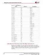
Page 29: ...rential signals such as LVDS data All differential signals are routed with 100Ω differential trace impedance Matched length traces are used across all differential signals Because the differential signals connect to the FPGA I O they may also be used as independent single ended nets The VCCIO of these signals can be set to 2 5V or 3 3V by setting jumper J16 Table 2 23 summarizes the differential c...

Page 30: ... W24 J5 Pin 52 W23 HDR2_52 J5 Pin 54 HDR2_54 Y23 J5 Pin 56 Y22 HDR2_56 J5 Pin 58 HDR2_58 Y26 J5 Pin 60 Y25 HDR2_60 J5 Pin 62 HDR2_62 AA26 J5 Pin 64 AA25 HDR2_64 Table 2 23 Expansion I O Differential Connections J5 Continued Header Pin Diff Pair Neg Label Diff Pair Neg FPGA Pin Diff Pair Neg Header Pin Diff Pair Pos FPGA Pin Diff Pair Pos Label Diff Pair Pos Table 2 24 Expansion I O Single Ended Co...

Page 31: ...pansion card Bi directional level shifting transistors allow the expansion card to utilize 2 5V to 5V signaling on the IIC bus Power supply connections to the expansion connectors provide ground 2 5V 3 3V and 5V power pins If the expansion card draws significant power from the SP 305 board the user must ensure that the total power draw can be supplied by the board The SP 305 expansion connector is...

Page 32: ...J3 Pin 9 VCC3V3 N A 3 3V Power Supply J3 Pin 10 HR3_10 A7 FPGA I O J3 Pin 11 FPGA_PROM_TMS N A Expansion TMS J3 Pin 12 FPGA_PROM_TCK N A Expansion TCK J3 Pin 13 EXPANSION_TDO N A Expansion TDO J3 Pin 14 FPGA_TDO N A Expansion TDI J3 Pin 15 HR3_15 G8 FPGA I O J3 Pin 16 HR3_16 B8 FPGA I O J3 Pin 17 HR3_17 A8 FPGA I O J3 Pin 18 HR3_18 G9 FPGA I O J3 Pin 19 HR3_19 D9 FPGA I O J3 Pin 20 HR3_20 G10 FPGA...

Page 33: ...vices the communication channel to the MCP2515 is through an SPI port See section 35B to set the jumpers in the right position to select either the CAN MAC PHY or just the CAN PHY Note When using the CAN controller There is an option to use the CAN MAC device or have the CAN MAC implemented in the FPGA To have the FOPGA drive the CAN PHY RX and TX signals that connect to the MPC2551 CAN PHY device...

Page 34: ...the CAN_RXCAN_MAC Reference Designator Jumper Pin CAN 16 Mhz Oscillator Socket 35c The SP305 has a Oscillator socket for a 16Mhz Oscillator CAN_CLK B7 CAN_SOF E6 CAN_TX0RTS D6 CAN_TX1RTS C6 CAN_TX2RTS B6 CAN_CS A3 CAN_SO C4 CAN_SI B4 CAN_SCK A4 CAN_INT C4 CAN_RESET A6 CAN_RX0BF B5 CAN_RX1BF A5 Table 2 27 MPC 2551 MAC Connections Reference Designator Label Definition FPGA Pin Table 2 28 FPGA and CA...

Page 35: ...a 32 bit data bus capable of running up to 266 MHz All DDR SDRAM signals are terminated through 47Ω resistors to a 1 25V VTT reference voltage The board is designed for matched length traces across all DDR control and data signals except clocks and the DDR Loop trace See the DDR Clock Signal and the DDR Loop Signal sections The board can support up to 256MB of total DDR SDRAM memory if larger chip...

Page 36: ...rovides high speed low latency external memory to the FPGA The memory is organized as 256K x 36 bits thereby providing for a 32 bit data bus with support for four parity bits Note The SRAM and FLASH memory share the same data bus Table 2 29 SRAM Label FPGA Pin Description SRAM_FLASH_D0 AD25 SRAM_FLASH_D1 AB22 SRAM_FLASH_D2 AC22 SRAM_FLASH_D3 AE24 SRAM_FLASH_D4 AF24 SRAM_FLASH_D5 AD23 SRAM_FLASH_D6...

Page 37: ...AM_FLASH_A0 AE15 SRAM_FLASH_A1 AF15 SRAM_FLASH_A2 AB16 SRAM_FLASH_A3 AC16 SRAM_FLASH_A4 AE17 SRAM_FLASH_A5 AA17 SRAM_FLASH_A6 AD17 SRAM_FLASH_A7 AD18 SRAM_FLASH_A8 AE18 SRAM_FLASH_A9 Y17 SRAM_FLASH_A10 AC17 SRAM_FLASH_A11 Y12 SRAM_FLASH_A12 AA14 SRAM_FLASH_A13 Y14 SRAM_FLASH_A14 AB15 SRAM_FLASH_A15 AD15 SRAM_FLASH_A16 AF17 SRAM_FLASH_A17 Y16 SRAM_FLASH_A18 AA16 SRAM_FLASH_A19 AB17 SRAM_FLASH_A20 W...

Page 38: ... 32 bit data bus that is shared with SRAM The reset for the AC97 Codec is shared with the reset signal for the flash memory chips and is designed to be asserted at power on or upon system reset Note The SRAM and FLASH memory share the same data bus SRAM_BW0 AF16 SRAM_BW1 AE16 SRAM_BW2 AA15 SRAM_BW3 W15 SRAM_AVD_LD_N W12 SRAM_CE1_N AC11 SRAM_FLASH_WE_N W11 SRAM_OE_N AF10 SRAM_ZZ AE10 SRAM_MODE AD10...

Page 39: ...M_FLASH_D15 AF21 SRAM_FLASH_D16 AB20 SRAM_FLASH_D17 AC20 SRAM_FLASH_D18 AE20 SRAM_FLASH_D19 AF20 SRAM_FLASH_D20 AA20 SRAM_FLASH_D21 Y19 SRAM_FLASH_D22 AA19 SRAM_FLASH_D23 AB19 SRAM_FLASH_D24 AC19 SRAM_FLASH_D25 AD19 SRAM_FLASH_D26 AE19 SRAM_FLASH_D27 AF19 SRAM_FLASH_D28 Y18 SRAM_FLASH_D29 AA18 SRAM_FLASH_D30 AB18 SRAM_FLASH_D31 AC18 FLASH_A0 AA10 Connected to Flash A0 SRAM_FLASH_A0 AE15 Connected ...

Page 40: ...7 SRAM_FLASH_A10 AC17 SRAM_FLASH_A11 Y12 SRAM_FLASH_A12 AA14 SRAM_FLASH_A13 Y14 SRAM_FLASH_A14 AB15 SRAM_FLASH_A15 AD15 SRAM_FLASH_A16 AF17 SRAM_FLASH_A17 Y16 SRAM_FLASH_A18 AA16 SRAM_FLASH_A19 AB17 SRAM_FLASH_A20 W16 SRAM_FLASH_A21 AC10 SRAM_FLASH_A22 AB10 Connected to Flash A23 FLASH_A23 Y10 Connected to Flash A24 FLASH_CE2 AF11 SRAM_FLASH_WE_N W11 FLASH_OE_N J2 FLASH_BYTE_N AD8 FLASH_AUDIO_RESE...

Page 41: ...4LC04B I ST is provided on the SP 305 board to store non volatile data such as an Ethernet MAC address The EEPROM write protect is tied off on the board to disable its hardware write protect The IIC bus utilizes 2 5V signaling and can operate at up to 400 kHz IIC bus pull up resistors are provided on the board The IIC bus is extended to the expansion connector so that the user may add additional I...

Page 42: ...IFF 42 The SP 305 board has an IFF Encryption device connected to an FPGA I O pin This IFF device can be interfaced to an FPGA design in such a way that the functionality of the design can be licensed or enabled by the authentication with the IFF device Label Description FPGA Pin IFF_FPGA One Wire Interface F7 Table 2 34 SPI Pin Connections ...

Page 43: ...rm Flash Select 1 17 J38 2 3 Platform Flash Enable and Reset Control 39 J26 1 2 Selects JTAG Connection Chain to Expansion Header default no header in JTAG Chain 25 J28 Connects Auxiliary Power to USB Port 21 J32 2 3 Selects between the USB Debug UART port and the UART1 SOUT 21 J33 2 3 Selects between the USB Debug UART port and the UART1 SIN SP305 Spartan 3 Development Platform User Guide 37 UG21...

Reviews: