44
VC707 Evaluation Board
UG885 (v1.2) February 1, 2013
Chapter 1:
VC707 Evaluation Board Features
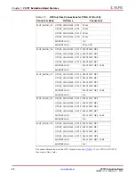
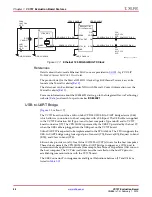
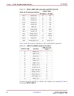
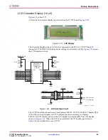
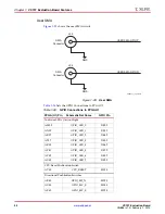
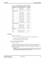
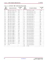
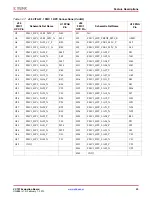
lists the connections between the FPGA and the LCD header.
References
The data sheet for the Displaytech S162DBABC LCD can be found at the Displaytech
website
S162D
model full spec download arrow.
I
2
C Bus
[
, callout
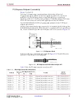
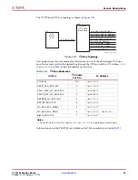
The VC707 board implements a single I
2
C port on the FPGA (IIC_SDA_MAIN,
IIC_SDA_SCL), which is routed through a 1-to-8 channel I
2
C bus switch (U52). The bus
switch can operate at speeds up to 400 kHz.
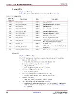
The bus switch I
2
C address is
0x74
(
0b01110100
) and must be addressed and configured
to select the desired downstream device.
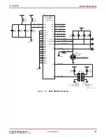
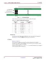
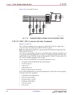
X-Ref Target - Figure 1-21
Figure 1-21:
LCD Header Details
UG885_c1_21_021412
LCD Display Assembly
VC707 PWA
10 mm
Low Profile Socket
Samtec SLW-107-01-L-D
Low Profile Terminal
Samtec MTLW-107-07-G-D-265
Table 1-23:
FPGA to LCD Header Connections
FPGA (U1)
Pin
Net Name
LCD Header Pin
(J31)
AT42
LCD_DB4_LS
4
AR38
LCD_DB5_LS
3
AR39
LCD_DB6_LS
2
AN40
LCD_DB7_LS
1
AR42
LCD_RW_LS
10
AN41
LCD_RS_LS
11
AT40
LCD_E_LS
9

