54
VC707 Evaluation Board
UG885 (v1.2) February 1, 2013
Chapter 1:
VC707 Evaluation Board Features
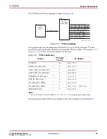
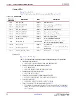
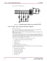
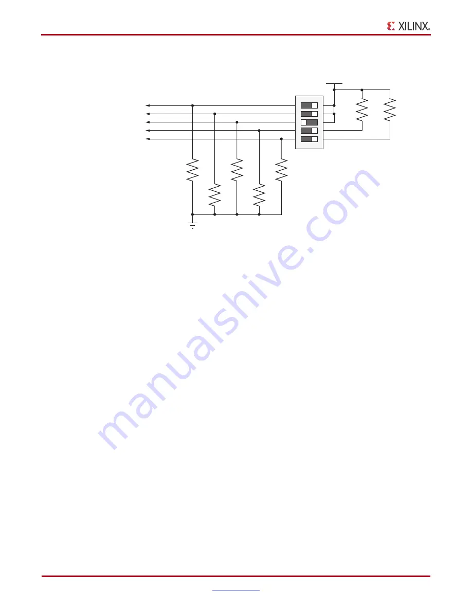
shows the SW11 circuit.
VITA 57.1 FMC1 HPC Connector (Partially Populated)
[
, callout
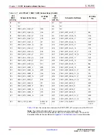
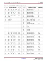
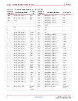
The VC707 board implements two instances of the FMC HPC VITA 57.1 specification
connector. This section discusses the FMC1 HPC J35 connector.
Note:
The FMC1 HPC J35 connector is a keyed connector oriented so that a plug-on card faces
away from the VC707 board.
The VITA 57.1 FMC standard calls for two connector densities: a high pin count (HPC) and
a low pin count (LPC) implementation. A 400 pin 10 x 40 position connector form factor is
used for both versions. The HPC version is fully populated with all 400 pins present. The
LPC version is partially populated with 160 pins.
The 10 x 40 rows of an FMC HPC connector provides pins for up to:
•
160 single-ended or 80 differential user-defined signals
•
10 GTX transceivers
•
2 GTX clocks
•
4 differential clocks
•
159 ground and 15 power connections
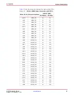
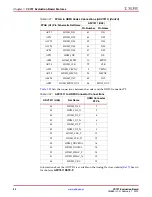
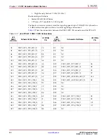
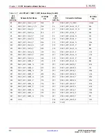
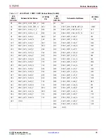
The VC707 board FMC1 HPC connector J35 implements a subset of the maximum signal
and clock connectivity capabilities:
•
80 differential user-defined pairs
•
34 LA pairs (LA00-LA33)
•
24 HA pairs (HA00-HA23)
•
22 HB pairs (HB00-HB21)
•
8 GTX transceivers
•
2 GTX clocks
X-Ref Target - Figure 1-32
Figure 1-32:
Configuration Mode and Upper Linear Flash Address Switch
UG885_c1_29_030512
SDA05H1SBD
SW11
R226
220
Ω
0.1 W
1%
R227
220
Ω
0.1 W
1%
VCC1V8
FPGA_M2
FPGA_M1
FPGA_M0
FLASH_A25
FLASH_A24
R341
1.21k
Ω
0.1 W
1%
R340
1.21k
Ω
0.1 W
1%
R339
1.21k
Ω
0.1 W
1%
R338
1.21k
Ω
0.1 W
1%
R337
1.21k
Ω
0.1 W
1%
1
2
3
4
5
10
9
8
7
6
GND


