VC707 Evaluation Board
71
UG885 (v1.2) February 1, 2013
Configuration Options
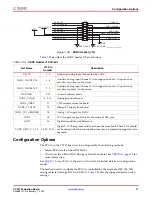
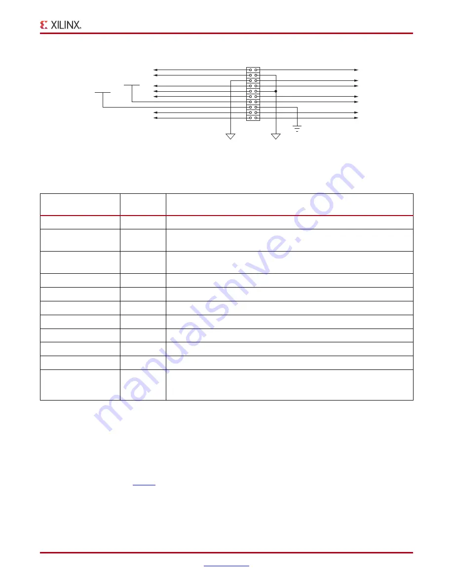
describes the XADC header J19 pin functions.
Configuration Options
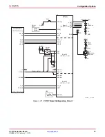
The FPGA on the VC707 board can be configured by the following methods:
•
Master BPI (uses the Linear BPI Flash).
•
JTAG (uses the USB-to-JTAG Bridge or Download cable). See
more information
See
7 Series FPGAs Configuration User Guide
for further details on configuration
modes.
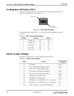
The method used to configure the FPGA is controlled by the mode pin (M2, M1, M0)
settings selected through DIP switch SW11.
lists the supported mode switch
settings.
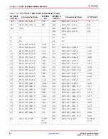
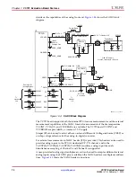
X-Ref Target - Figure 1-35
Figure 1-35:
XADC Header (J19)
UG885_c1_32_030512
XADC_VP
XADC_VAUX0N
XADC_VAUX8P
XADC_DXN
XADC_VCC_HEADER
XADC_VN
XADC_VAUX0P
XADC_VAUX8N
XADC_DXP
XADC_VREF
XADC_GPIO_0
XADC_GPIO_2
XADC_GPIO_1
XADC_GPIO_3
J19
1
3
5
7
9
11
13
15
17
19
2
4
6
8
10
12
14
16
18
20
GND
XADC_AGND
XADC_AGND
XADC_VCC5V0
VADJ
Table 1-33:
XADC Header J19 Pinout
Net Name
J19 Pin
Number
Description
VN, VP
1, 2
Dedicated analog input channel for the XADC.
XADC_VAUX0P, N
3, 6
Auxiliary analog input channel 0. Also supports use as I/O inputs when
anti-alias capacitor is not present.
XADC_VAUX8N, P
7, 8
Auxiliary analog input channel 8. Also supports use as I/O inputs when
anti-alias capacitor is not present.
DXP, DXN
9, 12
Access to thermal diode.
XADC_AGND
4, 5, 10
Analog ground reference.
XADC_VREF
11
1.25V reference from the board.
XADC_VCC5V0
13
Filtered 5V supply from board.
XADC_VCC_HEADER
14
Analog 1.8V supply for XADC.
VADJ
15
VCCO supply for bank which is the source of DIO pins.
GND
16
Digital Ground (board) Reference
XADC_GPIO_3, 2, 1, 0
19, 20, 17, 18
Digital I/O. These pins should come from the same bank. These I/Os should
not be shared with other functions because they are required to support 3-state
operation.


