Getting Started with the VC707 Evaluation Kit
11
UG848 (v1.4.1) October 14, 2015
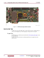
Built-In Self Test
Run BIST
1.
Complete the tasks under
.
2.
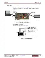
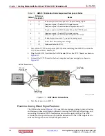
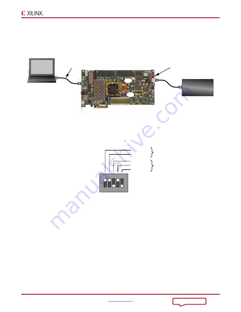
Connect the VC707 board to the host computer and power supply as shown in
3.
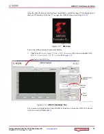
Turn board power on (SW12).
4.
Set DIP switch SW11 as shown in
X-Ref Target - Figure 1-7
Figure 1-7:
BIST Board Connections
UG
8
4
8
_c1_06_040314
Power
Su
pply
100VAC–240VAC Inp
u
t
12 VDC 5.0A O
u
tp
u
t
To J1
8
Bo
a
rd Power
S
witch
S
W12
Ho
s
t
Comp
u
ter
U
S
B c
ab
le
s
t
a
nd
a
rd-A pl
u
g
to mini-B pl
u
g
S
W11
To J17
(UART l
ab
el)
S
W9
X-Ref Target - Figure 1-8
Figure 1-8:
SW11 BIST Settings
UG848_c1_07_062112
SW11
1 2 3 4 5
FPGA_M0
0 (Off)
FPGA_M1
FPGA_M2
FLASH_A24
FLASH_A25
1 (On)
Pin 1
Upper Flash ADDR = 0b11
points to the BIST bitstream
in BPI flash memory at U3
Master BPI Mode = 0b010
configures FPGA from
BPI flash memory at U3
Summary of Contents for VC707
Page 24: ...Printed in Singapore...

