Getting Started with the VC707 Evaluation Kit
9
UG848 (v1.4.1) October 14, 2015
Preliminary Setup
Verify Jumpers are in Default Positions
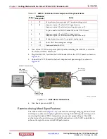
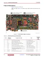
Verify the jumpers on the VC707 board are positioned as shown in
for the location of the jumpers.
Table 1-1:
Default Jumper Settings
Callout
Jumper
Function
Default Jumper
Position
Schematic
0381418 Page
Number
1
J6
SFP Enable
None
31
2
J9
XADC GND ferrite filter bypass jumper
None
40
3
J10
XADC GND-to-XADC_AGND jumper
1–2
40
4
J11
TI Controller U42 Addr 52 Reset jumper
None
46
5
J12
TI Controller U43 Addr 53 Reset jumper
None
50
6
J13
USB Mini-B Connector J2 VBUS
None
44
7
J14
USB SMBC U8 CLKOUT selector
None
44
8
J38
SFP RX Rate: 1-2 = Full BW Rate, 2-3 = Low BW Rate
1–2
31
9
J39
SFP TX Rate: 1-2 = Full BW Rate, 2-3 = Low BW Rate
1–2
31
10
J42
XADC external 1.2V or internal VREFP selector
1–2
40
11
J43
XADC VCC Select Header
2–3
40
12
J44
USB Mini-B Connector J2 GND jumper
None
44
13
J45
USB SMBC U8 VBUS
1–2
44
14
J49
PCIe Bus Width Select Header
1-2
30
15
J50
TI Controller U64 Addr 54 Reset jumper
None
53
16
J51
FMC_VADJ_ON_B jumper
1–2
46
17
J53
XADC VCC5V0-to-XADC_VCC5V0 jumper
1–2
40
18
J54
XADC REF3012 U35 V
IN
Select
1–2
40
Summary of Contents for VC707
Page 24: ...Printed in Singapore...


