Virtex-6 FPGA System Monitor
47
UG370 (v1.1) June 14, 2010
Application Guidelines
The reference inputs should be routed as a tightly coupled differential pair from the
reference IC to the package pins. If routed on the same signal layer, the supply and analog
ground traces (AV
DD
and AV
SS
) should be used to shield the reference inputs because they
have a higher tolerance to any coupled noise.
External Analog Inputs
The analog inputs are high-impedance differential inputs. The differential input scheme
enables the rejection on common mode noise on any externally applied analog-input
signal. Because of the high impedance of each input (such as V
P
and V
N
), the input AC
impedance is typically determined by the sensor, the output impedance of the driving
circuitry, or other external components.
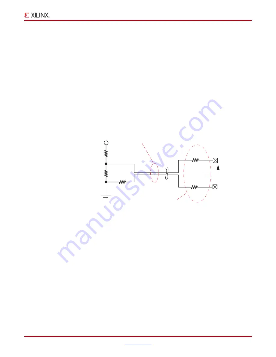
illustrates a simple example where a
simple resistor divider network is used to monitor an external 2.5V supply rail in unipolar
input mode (see
). To ensure that noise coupled onto the analog inputs is
common to both inputs (reduce differential noise), the impedance on each input should be
matched. Analog-input traces on the PCB should also be routed as tightly coupled
differential pairs.
Anti-Alias Filters
, is a low-pass filter network at the analog differential inputs. This
filter network is commonly referred to as the
anti-alias
filter and should be placed as close
as possible to the package pins. The sensor can be placed remotely from the package as
long as the differential input traces are closely coupled. The anti-alias filter attenuates high
frequency signal components entering the ADC where they could be sampled and aliased,
resulting in ADC measurement corruption. A discussion of aliasing in sampled systems is
beyond the scope of this document. A good data-converter reference book provides more
information on this topic.
PC Board Design Guidelines
illustrate one possible way to address the requirements outlined in
the previous sections.
shows how, by staggering the vias with respect to the
pads,
north-south
and
east-west
routing channels through the via field are created. These
routing channels can be used to bring tightly coupled differential pairs into the center of
the via field—even when using 5 mil tolerances.
X-Ref Target - Figure 26
Figure 26:
Voltage Attenuation Example
0.5V
10 nF
1 k
Ω
1 k
Ω
V
AUXP[x]
V
AUXN[x]
Place Anti-Alias Filters
Close to Package Pins
Tightly Coupled Routing
(long traces) for V
AUXP
and V
AUXN
+2.5V
5 k
Ω
4 k
Ω
20 k
Ω
UG370_26_060809
www.BDTIC.com/XILINX


