20
Virtex-6 FPGA System Monitor
UG370 (v1.1) June 14, 2010
Register File Interface
Test Registers (
43h
to
47h
)
These registers are intended for factory test purposes only and have a default status of
zero. The user must not write to these registers.
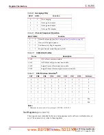
Table 8:
Averaging Filter
AVG1
AVG0
Function
0
0
No averaging
0
1
Average 16 samples
1
0
Average 64 samples
1
1
Average 256 samples
Table 9:
Channel Sequencer Operation
SEQ1 SEQ0
Function
0
0
Default safe mode
(see
Pre-Configuration Operation, page 10
)
0
1
One pass through sequence
1
0
Continuous cycling of sequence
1
1
Single Channel mode (Sequencer Off)
Table 10:
Calibration Enables
Name
Description
CAL0
ADC offset correction enable
CAL1
ADC offset and gain correction enable
CAL2
Supply Sensor offset correction enable
CAL3
Supply Sensor offset and gain correction enable
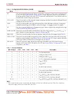
Table 11:
DCLK Division Selection
(1)
CD7
CD6
CD5
CD4
CD3
CD2
CD1
CD0
Division
0
0
0
0
0
0
0
0
2
0
0
0
0
0
0
0
1
2
0
0
0
0
0
0
1
0
2
0
0
0
0
0
0
1
1
3
0
0
0
0
0
1
0
0
4
–
–
–
–
–
–
–
–
..
.
1
1
1
1
1
1
1
0
254
1
1
1
1
1
1
1
1
255
Notes:
1. Minimum division ratio is 2, for example, ADCCLK = DCLK/2.
www.BDTIC.com/XILINX


