40
Virtex-6 FPGA System Monitor
UG370 (v1.1) June 14, 2010
Analog Inputs
The dedicated ADC (V
P
and V
N
) and auxiliary analog inputs (V
AUXP
[15:0] and
V
AUXN
[15:0]) can be driven from either unipolar or bipolar sources. When driving the
analog inputs from a bipolar source, the inputs must be used in a bipolar mode (see
). Unipolar and bipolar mode selection is made by writing to configuration
register 0 (see
).
Auxiliary Analog Inputs
The auxiliary analog inputs (V
AUXP
[15:0] and V
AUXN
[15:0]) are analog inputs shared with
regular digital I/O package pins. These analog inputs have a lower input bandwidth than
the dedicated analog input channel (V
P
/V
N
)
The auxiliary analog input can be enabled as analog inputs preconfiguration only via the
JTAG TAP (see
). To enable all 16 auxiliary analog input
channels in preconfiguration operation, a
1
must be written to bit 0 of the register at
address
02h
(V
CCAUX
status register) in the System Monitor register file interface. The
internal mapping in the System Monitor enables the auxiliary channels using the JTAG
interface.
The auxiliary analog inputs are automatically enabled when System Monitor is
instantiated in a design, and these inputs are connected in the instantiation. Only the
auxiliary inputs connected in a design are enabled as analog inputs. The System Monitor
auxiliary input pins are defined in
Virtex-6 FPGA Packaging and Pinout Specification
as
_SMxP_
and
_SMxN_,
where
x
is the auxiliary pair number. For example, the auxiliary
input V
AUXP
[15] is designated IO_L10P_CC_SM15P_11 in the pinout specification.
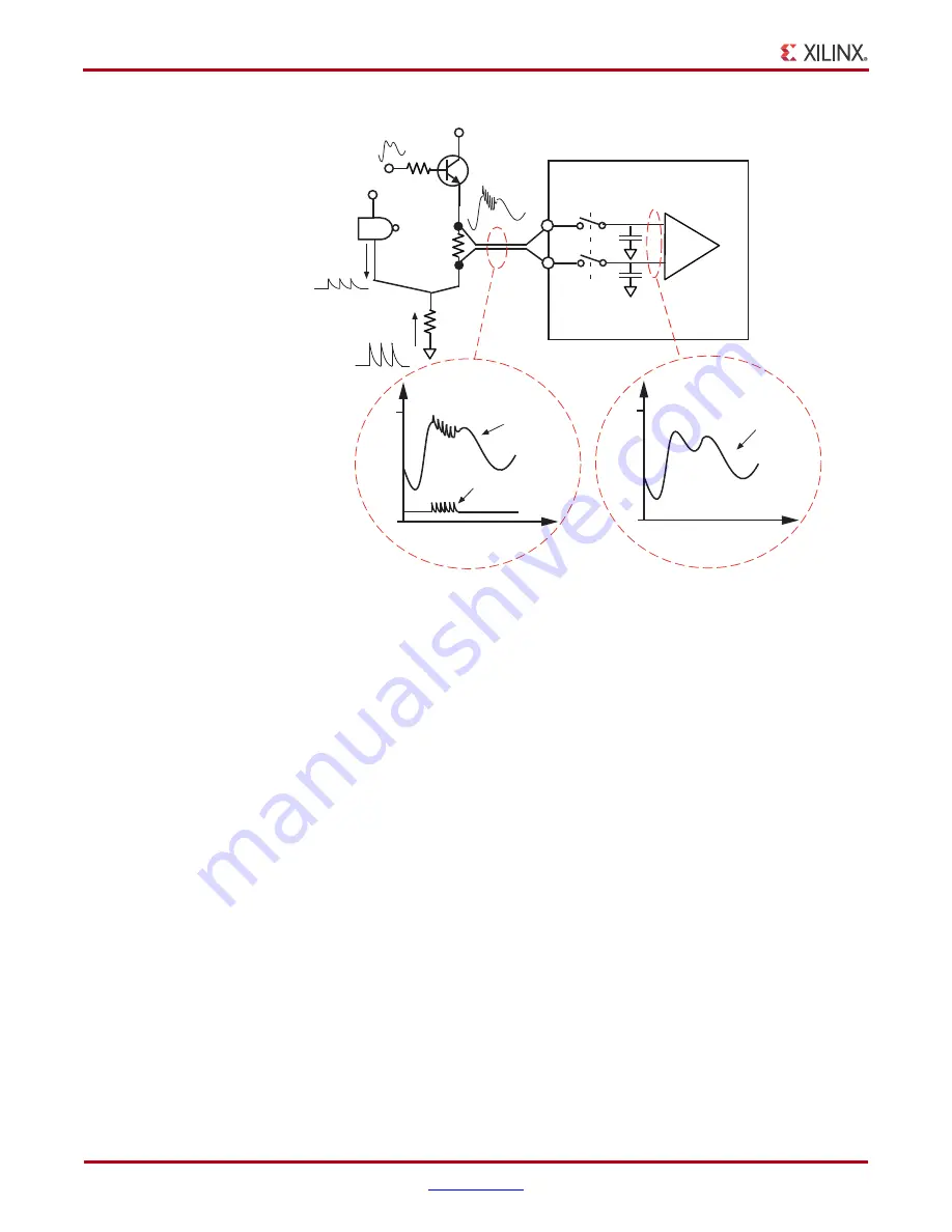
X-Ref Target - Figure 17
Figure 17:
Differential Sampling Scheme Rejects Common Mode Noise
Noise
Current
T/H
V
P
V
N
Note 1: RG is Common Ground Impedance.
R
G
(!)
Differential
Common Mode
Rejection removes
noise
Sampling
0V
1V
V
P
V
N
0V
1V
V
P
– V
N
Common Noise
on V
P
and V
N
+
–
UG370_17_060809
Noise
Voltage
www.BDTIC.com/XILINX


