Spartan-3A DSP 3400A Edition User Guide
www.xilinx.com
41
UG498 (v2.2) November 17, 2008
Spartan-3A DSP 3400A Edition Board Hardware
R
FMC Expansion Connectors
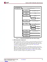
The FMC expansion connectors (J13 and J19) follow the VITA 57.1 FMC standard (standard
to be released at a later date) and are used in low-pin-count (LPC) format. The Spartan-3A
DSP 3400A Edition board was designed with a preliminary version of the standard.
When an FMC mezzanine module is intended to be used, the FPGA should access the FMC
mezzanine module's I
2
C EEPROM to read the board information. This information allows
the FPGA to set the appropriate I/O voltages to the FPGA I/Os connected to the FMC
expansion connector. The way the board information will be stored in the FMC mezzanine
I
2
C EEPROM is not defined at this time. A work group is currently developing the Vita-
57.2 standard. The standard should be released soon.
To set the appropriate voltage on the FMC connector, an I
2
C digital pot must be set to a
specific value. The value should be written to the volatile register of the digital pot. This
register is located at address 0x00 for FMC connector #1 and to address 0x01 for FMC
connector #2. To write to the volatile section of the digital pot make sure that address 0x08
is set to 0x80.
Use the following steps to configure the digital pot to the appropriate voltages:
Vout = 1.5V
1.
Configure register 0x8 to value 0x80
2.
Configure register 0x0 (FMC #1) or 0x1 (FMC #2) to value 0x8A
Vout = 1.8V
1.
Configure register 0x8 to value 0x80
2.
Configure register 0x0 (FMC #1) or 0x1 (FMC #2) to value 0x57
Vout = 2.5V
1.
Configure register 0x8 to value 0x80
2.
Configure register 0x0 (FMC #1) or 0x1 (FMC #2) to value 0x1E
Vout = 3.3V
1.
Configure register 0x8 to value 0x80
2.
Configure register 0x0 (FMC #1) or 0x1 (FMC #2) to value 0x00
DDR2 Memory
DDR2 Memory Expansion
The SODIMM connector lets you install DDR2 SODIMM modules with more memory
because higher order addresses and chip select signals are also routed from the SODIMM
connector to the FPGA. However, a permanent limitation is that only the first 32 bits of
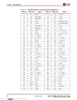
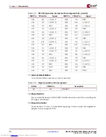
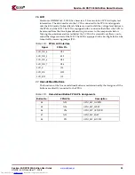
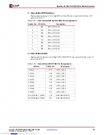
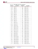
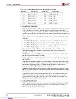
data are routed to the FPGA, as shown in
Table 1-28
.
DDR2 Clock Signal
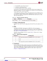
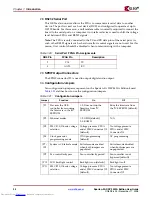
Two matched-length pairs of DDR2 clock signals are broadcast from the FPGA to the
SODIMM connector. The FPGA design is responsible for driving the two clock pairs at a
low skew. The delay on the clock traces is designed to match the delay of the other DDR2
control signals.
electronic components distributor

