42
www.xilinx.com
Spartan-3A DSP 3400A Edition User Guide
UG498 (v2.2) November 17, 2008
Chapter 1:
Introduction
R
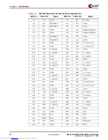
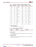
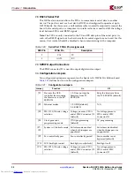
DDR2 Signaling
All DDR2 control signals are terminated through 47-? resistors to a 0.9-V VTT reference
voltage. The DDR2 interface of the FPGA supports SSTL18 signaling and all the DDR2
signals are controlled impedances. The DDR2 data, mask, and strobe signals are of
matched length within byte groups. On die termination (ODT) is available and better
performance can be achieved when used by the memory controller.
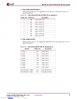
MIG Compatibility
MIG can be used to generate a compatible design for the Spartan-3A DSP 3400A Edition
board.
I
2
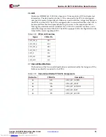
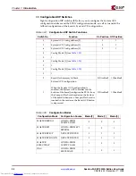
C Bus Addressing
The Spartan-3A DSP 3400A Edition board uses an I
2
C bus to interface different devices to
the FPGA. Because of the large amount of devices having similar slave address, an I
2
C
MUX (Philips PCA9544APW) is used to separate those devices from one to the other.
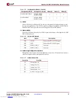
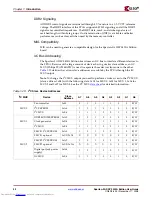
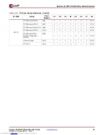
Table 1-29
defines the various slave addresses accessible by the FPGA through the I
2
C
MUX output.
Note
: To change the I
2
C MUX output you need to perform a write access to the I
2
C MUX
(slave address 0xE4) with the following data: 0x04 for MUX 0, 0x05 for MUX 1, 0x06 for
MUX 2 and 0x07 for MUX3. See the I
2
C MUX
data sheet
for detailed information.
Table 1-29:
I
2
C Slave Device Addresses
I
2
C MUX
Device
Slave
Address
A7
A6
A5
A4
A3
A2
A1
A0
MUX 0
Fan controller
0x58
0
1
0
1
1
0
0
R/W
I
2
C EEPROM
0xA8
1
0
1
0
1
0
0
R/W
I
2
C MUX
0xE4
1
1
1
0
0
1
0
R/W
MUX 1
DDR2 SODIM EEPROM 0xA0
1
0
1
0
0
0
0
R/W
Clock generator
0xD4
1
1
0
1
0
1
0
R/W
I
2
C MUX
0xE4
1
1
1
0
0
1
0
R/W
MUX 2
FMC #1 I
2
C EEPROM
0xA0
1
0
1
0
0
0
0
R/W
FMC #1 optional
0xX0/0xX8
X
X
X
X
X
0
0
R/W
FMC #2 I
2
C EEPROM
0xA2
1
0
1
0
0
0
0
R/W
FMC #2 optional
0xX2/0xXA
X
X
X
X
X
0
1
R/W
Digital pot (adj. power
supply)
0xA4
1
0
1
0
0
1
0
R/W
I
2
C MUX
0xE4
1
1
1
0
0
1
0
R/W
electronic components distributor

