background image

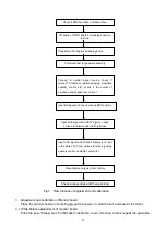
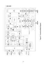
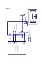
Short introduction and working principle of    LC-30K9A(W)/LC-40K9A 

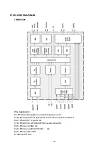
This type series of the machine set takes the form of STB plus MONITOR. Without STB, it is a 

standard computer monitor. With STB, it is a CTV receiver with powerful functions.   

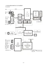
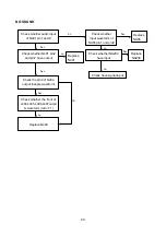
For work principle flow of this series, refer to block diagram of a complete set. 

The RF signal of broadcast TV, with the help of tuner TUNA02, turns out color full TV signal TV-IN2 

and second sound IF signal. The RF signal of satellite TV with the help of BS tuner TUNA01, produces 
color full TV signal TV-BS and left and right sound signal R/L. TV video signal of TV-IN2 and TV-BS after 
the selection by PI50V330(U40-1) is sent to video decoder VPC3230(U29). The YcbCr and PCMCIA 
input from commuter board and the YUV after selection in U40-2 are also sent to U29 respectively. 
Furthermore AV1/SVHS,AV2 are also sent to U29. After the selection of above four video signals are 
subject to selection and decoding in U29 and then sent in format of 8 bi ITU-R656 to FLI2310(U13)for 
progressive treatment. One route of the video signal that is subject to selection in U29 is sent to output 
through AV.   

Two routes of D4 signal, YpbPr, after the selection in BA7657F(U11), are sent to MST9883(U30), 

where they are sent, after A/D conversion, to U13 in the format of 24 bit YUV.   

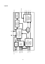
24bit RGB signal is output and sent to main processing chip JAG-ASM(U12) after the above two 

routes of signal are processed in terms of matrix, color density, and tint in U13. RGB signal of computer 
VGA is also sent to U12, where the two routes of signal are subject to selection and processing for 
picture format. One route RGB signal of VGA undergoes A/D conversion before being subject to 
selection and digit display processing together with another route of signal, including OSD, GAMMA 
calibration, brightness and contrast processing. These signals are changed into the format of 1024*768 
and output in 24 bit RGB signal. This signal is then converted into DVI signal(four pairs of differential 
signal) in SiI170 and sent to MONITOR. 

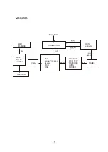
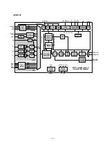
In MONITOR, four pairs of differential signal from STB are sent to PW131(N301). As there is also 

VGA input terminal in N301, the two signals, after the selection and formatting, output to output in 48bit 
RGB signal and sent to LVDS converter DS90C383(N201, N202), where they are converted to four pairs 
of low voltage differential signals and then send to LCD screen for picture display.       

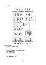
The audio signal of left and right sound channels D4, YCBCR and PCMCIA undergoes selection in 

HEF4052(U34), and is then sent to MSP3420(NA04). AV1/SVHS and AV2, after  selection in 
HEF4052(U34), is sent to NA04 together with SIF of TUNA02 and R/L of TUNA01    as well as R/L of 
VGA two tuners and R/F of VGA. In NA04, SIF is demodulated into audio signal before being switched 
for selection with other four routes of R/L signal. The selected R/L after the processing in volume and 
sound effect is then output as follows: three R/L routes for left and right sound channels, one route for AV 
OUT, and another route for M62494(N203)of SRS sound field processor for SRS processing. The signal 
output to left and right sound channels is sent to MONITOR, and after sound power amplification in 
LX1722(N404), is for driving the speaker. The last route, after power amplification of earphone in 
TLE2142, is for driving the earphone.   

The power supply is through an adaptor, where it is converted to different power supplies required 

by monitor and STB. 


Summary of Contents for LC-30K9A(W)

Page 1: ...COLOR TELEVISION LC 30K9A W LC 40K9A...

Page 2: ...Trouble shooting Principle analysis of L30K9A w and 40K9A BLOCK DIAGRAM Wiring diagram Serial No of Parts Identification criteria for the bright spot and dark spot of the LCD screen Troubleshooting gu...

Page 3: ...chen or nearby fire source heating equipment and devices or exposure to sunlight etc Otherwise bad effect will result 2 5 If any foreign substance such as water liquid metal slices or other matters ha...

Page 4: ...as commmonly called ghost shadow The extent of the residual picture varies with the maker of LCD screen This phenonmenon doesn t represent failure This ghost shadow may remain in the picture for a pe...

Page 5: ...o central signal source check if various TV functions station skipping modulate quantity control etc check if the output of earphone and speaker are normal Combined test for general assembly Input AV...

Page 6: ...that of the seventh grade to 400nit Fix B CUT and B DRV at 128 Adjust R G CUT to set the second color coordinates to 270 283 Adjust R G DRV to set the seventh grade color coordinates to 270 283 Repeat...

Page 7: ...over Adjust the value of Option to 9 S bright to 124 S contrast to 140 4 3 2 White balance adjustment of TV channel Input AV signal PM5518 grey grade signal enter the adjustment menu of white balance...

Page 8: ...e broadcast signal itself is not good Check if the outdoor antenna is disconnected Check if the antenna is correctly oriented Fringe in picture Check if the antenna is correctly oriented Maybe there i...

Page 9: ...e liquid crystal TV set and make proper adjustment according to the signal types Picture too bright and there is distortion in the brightest area Check if the contrast setting is too high Possibly the...

Page 10: ...ected Check if the cable connection is loose When playing VHS picture search tape there are lines at the top or bottom of the picture When being played or in pause VHS picture search tape sometimes ca...

Page 11: ...te RGB signal of VGA undergoes A D conversion before being subject to selection and digit display processing together with another route of signal including OSD GAMMA calibration brightness and contra...

Page 12: ...U2 MICRO CONTRLER TSC80251G2D U4 FLASHMEMORY IR SIF AV1 SVHS R L AV2 R L D4 1 R L D4 2 R L VGA R L PCMCI R L AV R L OUT NA04 AUDIO PROCESSOR MSP3420 U34 HEF4052 NA05 SRS 3D STEREO CONTROLLER M62494 N...

Page 13: ...OR N401 M62429E N404 LX1722 Amplifier SPEAKER VGA N301 Image Processor Scaler MCU OSD DC IN connector PANEL DXE N201 DXO N202 DS90C383 LVDS DRIVER BOX power monitor power lamp panel 2 x 4 48bit R L DV...

Page 14: ...the operation of IC 27 28 PIN output left and right sound channel R L to speaker processor 36 37 PIN AV OUT of sound R L 47 48 PIN D4 1 D4 2 PCMCIA YCbCr selected input R L 50 51 PIN Input of VGA R L...

Page 15: ...PIN Input Y of PCMCIA YCbCr 6 PIN Input V of PCMCIA YCbCr 31 34 37 40 PIN output format signal of ITU R656 70 PIN Video of AV OUT 71 PIN Input C of SVHS 72 PIN input Video SVHS in priority of Y or AV...

Page 16: ...ortA 7 0 GPIO PWM IR Decoder A 19 1 D 15 0 CS 1 0 2 Wire Serial Microprocessor Bus Display Timing Generator Memory Out Bus Memory Buffer Processor Memory Interface Memory In Bus OSD VYUV 7 0 VCLK VPEN...

Page 17: ...15 4 JAG ASM...

Page 18: ...16 5 SiI170...

Page 19: ...17 6 LX1722...

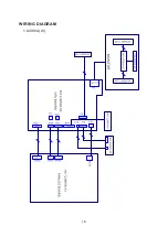
Page 20: ...18 WIRING DIAGRAM 1 L30K9A W...

Page 21: ...19 2 L40K9A...

Page 22: ...353 80251 10 Self produced Infra red receive assy 667 L30K9 09 667 L40D9 09 Self produced KEY board assy 667 L30K9 05 Self produced PCMCIA board assy 667 L40D9 90 N8 ES6420 353 64200 20 Self produced...

Page 23: ...mm 5mm Total defected point 8 7 5 4 Notes 1 Definition of defected point bright spot dark spot It is identified as a defected point if its area exceeds 1 2 of a single picture element R G B 2 Definiti...

Page 24: ...CK LIGHT ON Back light off no no normal normal no no Check whether power supply IC Check power supply circuit and IC Check whether N205 pin3 the voltage changing low level Replace N205 No screen displ...

Page 25: ...waveform of NA05 pin1 and pin2 Check whether N401 pin2 and pin7 have output Check the pin2 of N404 output triangle waveform Check whether the front of L404 L405 L406 L407outpu ts waveform ratio 1 1 R...

Page 26: ...est U38 waveform from TXC TX0 TX2 Test whether U38 power supply 3 3V Test wether U38 pin2 pin4 pin5 pin57 waveform Check path turned 5V into 3 3v Replace U38 Test whether power supply 1 5v 2 5v 3 5v C...

Page 27: ...ture Enter factory adjustment menu execute CLEAR EEPROM after operation shut off and re put on to check if there is a picture change CPU board Calibrate CPU board Replace CPU board Screen display NO S...

Page 28: ...1 2 5 4 6 7 8 9 10 13 14 15 16 19 20 21 22 23 24 25 26 27 32 33 34 35 36 37 38 39 40 41 42 12 11 3 17 18 28 29 30 31 L30K9A W EXPLODED VIEWS...

Page 29: ...grille right 13 loudhailer left 34 speaker s front cover right 12 socket wp2 9c left 33 loudhailer right 11 speaker s front cover left 32 socket wp2 9c right 10 speaker grille left 31 speaker s front...

Page 30: ...1 2 3 4 5 6 7 8 9 10 11 12 13 14 15 16 17 18 19 20 21 22 23 24 25 26 27 28 29 30 31 33 34 35 36 37 38 32 LC40K9A EXPLODED VIEWS...

Page 31: ...tor board 12 pnael connect parts left 33 shielding board 11 screw 32 shielding board 10 LED column 31 shielding cover 9 wall connect parts 30 shielding cover 8 transition parts B 29 socket 7 pnael con...

Page 32: ...L30K9A W SCH...

Page 33: ......

Page 34: ......

Page 35: ......

Page 36: ......

Page 37: ......

Page 38: ......

Page 39: ......

Page 40: ......

Page 41: ......

Page 42: ......

Page 43: ......

Page 44: ......

Page 45: ......

Page 46: ......

Page 47: ......

Page 48: ......

Page 49: ......

Page 50: ...L40K9A SCH...

Page 51: ......

Page 52: ......

Page 53: ......

Page 54: ...F CB27 0 1UF CB16 0 1UF 1 2 CB47 100UF CB55 0 1UF CB17 0 1UF CB37 0 1UF R24 0 OHM 1 2 CB23 100UF CB40 0 1UF IN 3 OUT 2 ADJ 1 N13 2830 3 3V CB36 0 1UF CB4 0 1UF CB5 0 1UF 1 2 CB22 10UF 1 2 X2 Power 1 2...

Page 55: ...R22 33OHM D0 3 D1 4 D2 7 D3 8 D4 13 D5 14 D6 17 D7 18 OC 1 CLK 11 Q0 2 Q1 5 Q2 6 Q3 9 Q4 12 Q5 15 Q6 16 Q7 19 N2 74HCT374 V1 FDN338P 1 2 C5 100UF 1 2 C7 47UF C8 0 1UF C14 0 1UF C12 0 1UF R11 10K V2 F...

Page 56: ...LA18 LA4 LA2 LA9 LD6 LD5 LD7 LD0 RST LA5 LA16 LA17 LA11 LA10 LD3 LD1 LA13 LA15 LA3 LA8 LA0 LA21 LA19 LA6 LD4 LA12 LA7 LA1 LD2 LA14 LD 0 7 LA 0 19 LD 0 7 A0 12 A1 11 A2 10 A3 9 A4 8 A5 7 A6 6 A7 5 A8 2...

Page 57: ...DMA7 62 DMA8 63 DMA9 64 DMA10 65 DMA11 66 VSS 67 DCAS 69 DSCK DOE 70 DWE 71 DRAS0 72 DBANK0 DRAS1 73 DBANK1 DRAS2 74 VSS 76 DB0 77 DB1 78 DB2 79 DB3 80 DB4 81 DB5 82 VSS 84 DB6 85 DB7 86 DB8 87 DB9 8...

Page 58: ......

Reviews: