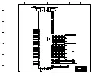
1
2
3
4
A
B
C
D
4
3
2
1
D
C
B
A
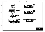
CNTLA
TWS-
MCLK-
CSB
CNTLB
CNTLC
ML
ZERO
MC
MD
TSD0-
TBCK-
R
L
R
L
DVDD
8
DGND
7
CSB/WO
23
MLIIS
28
MCDM1
27
MDDM0
26
MUTEB
25
MODE
24
LRCIN
1
DIN
2
BCKIN
3
XTI
5
VMID
18
ZERO
21
VOUTL
16
VOUTR
13
AGND
14
VREFN
19
VREFP
20
AVDD
15
N1
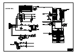
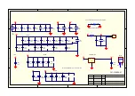
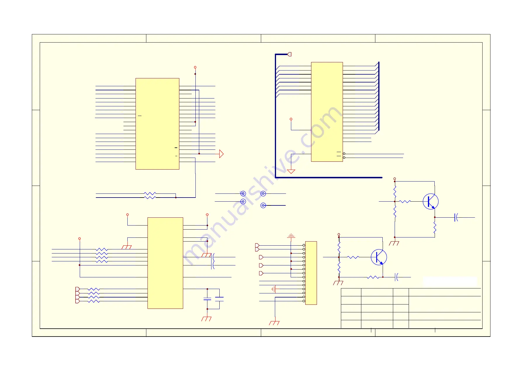
WM8706
R3
33 OHM
R4
33 OHM
C3
0.1UF
R8
33 OHM
1
2
C4
10UF
R10
33 OHM
R5
33 OHM
C1
10UF
R6
33 OHM
R7
33 OHM
C2
10UF
R9
33 OHM
VCCA
VCCA
VCCA
TSD0
MCLK
TWS
TBCK
VSYNC
HSYNC
UDAC
CDAC
YDAC
WOLFSON 2-CHANNEL AUDIODAC
2-CHANNEL AUDIO OUT
UDAC
YDAC
CDAC
1
2
3
4
5
6
7
8
9
10
11
12
13
14
15
X1
PORT
PHOTO_EN#
IR_DATA
LCS3#
LA4
LA8
LA3
LOE#
LA13
LCS2#
LD2
LA2
LA11
LA7
LD5
LA17
LA1
LA15
LA5
LA9
LD7
LD0
LA14
LA12
LD3
LA18
LD1
LD4
LA16
LD6
LA10
LA6
LA19
WRLL#
LA0
R54
OPEN 0
R55
0 OHM
VCC33
LA18
LA4
LA2
LA9
LD6
LD5
LD7
LD0
RST#
LA5
LA16
LA17
LA11
LA10
LD3
LD1
LA13
LA15
LA3
LA8
LA0
LA21
LA19
LA6
LD4
LA12
LA7
LA1
LD2
LA14
LD[0..7]
LA[0..19]
LD[0..7]
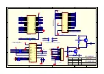
A0
12
A1
11
A2
10
A3
9
A4
8
A5
7
A6
6
A7
5
A8
27
A9
26
A10
23
A11
25
A12
4
A13
28
A14
29
A15
3
D0
13
D1
14
D2
15
D3
17
D4
18
D5
19
D6
20
D7
21
A16
2
CE
22
OE
24
A18
31
A17
30
A19
1
VCC
32
GND
16
N9
OPEN 27C040/080-90
VCC
LD[0..7]
4-PIN EXTENSION FOR ROM EMULATOR INTERFACE
4MBIT EPROM/FLASH
8MBIT EPROM
LCS3#
LOE#
WRLL#
LA20
TP4
TP2
TP1
TP3
HSYNC
VSYNC
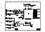
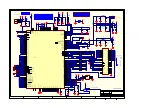
A16
1
A15
2
A14
3
A13
4
A12
5
A11
6
A9
7
A8
8
W
9
NC
10
NC
11
NC
12
A18
13
A7
14
A6
15
A5
16
A4
17
A3
18
A2
19
A1
20
A0
21
E
22
VSS
23
G
24
D0
25
D1
26
D2
27
D3
28
NC
29
VDD
30
VDD
31
D4
32
D5
33
D6
34
D7
35
A10
36
A19
37
NC
38
VSS
39
A17
40
N6
SST39VF080
V6
847
V7
847
R30
15k
R32
33k
R34
15k
R36
33k
R35
1k
R33
1k
R28
620
R37
620
C16
10uF
C17
10uF
VCCA
VCCA
R_OUT
L_OUT
L_OUT
R_OUT
Cr
Cb
Y
5
PCMCIA
782-L40D9-9000
203-L30K90-03
Summary of Contents for LC-30K9A(W)
Page 1: ...COLOR TELEVISION LC 30K9A W LC 40K9A...
Page 17: ...15 4 JAG ASM...
Page 18: ...16 5 SiI170...
Page 19: ...17 6 LX1722...
Page 20: ...18 WIRING DIAGRAM 1 L30K9A W...
Page 21: ...19 2 L40K9A...
Page 32: ...L30K9A W SCH...
Page 33: ......
Page 34: ......
Page 35: ......
Page 36: ......
Page 37: ......
Page 38: ......
Page 39: ......
Page 40: ......
Page 41: ......
Page 42: ......
Page 43: ......
Page 44: ......
Page 45: ......
Page 46: ......
Page 47: ......
Page 48: ......
Page 49: ......
Page 50: ...L40K9A SCH...
Page 51: ......
Page 52: ......
Page 53: ......
Page 58: ......


