background image

1

2

3

4

5

6

7

8

A

B

C

D

8

7

6

5

4

3

2

1

D

C

B

A

MA9

DMA3

LA18

MA4

LD7

DMA6

MA4

DB9

LD5

LA8

DB8

LA6

BANK0

MA8

YUV0

DB12

MA7

MA3

DB2

DMA10

YUV4

MA7

DMA0

XOUT

DB1

27MHZ

DB14

MA2

MA5

DB4

MA1

LA10

LD6

LA1

DB0

DQMX

DB7

DB5

MA9

DB14

DB6

LA11

MA10

DMA8

DMA11

LD3

LD1

LA9

YUV5

DB15

DMA4

DMA2

DMA9

DB7

MA11

DB3

LA12

MA5
MA6

DMA7

LA3

MA10

YUV2

LA17

YUV3

DB11

DB10

MA6

DB10

DB15

DB5

DB8

MA11

WE#

DMA1

AUX4

LA15

BANK1

LA7

LD4

XIN

LA0

CKE

DB2

DB3

RST#

LA4

CS0#

MA0

MA8

DB13

LA21

CAS#

DB11

WRLL#

LCS3#

DB13

LA19

DB12

LA13

MA3

DB1

EAUX31

DB6

DB4

DB9

RAS0#

LA5

LA2

MA2

MA1

LA16

LOE#

YUV1/VREF

LD0

DB0

DMA5

LD2

LA14

MA0

HRD#

HD3

HWR#

HD0

HA1

HD2

HD7

HD6

EAUX30

HSYNC

LCS2#

HD1

HD4
HD5

HA2

HIRQ

HA0

HD9
HD10
HD11

HD13
HD14
HD15

HRST#

HCS3#

HCS1#

27MHZ

LD[0..7]

DB[0..15]

HD[0..15]

HD12

WRHL#

LD8
LD9
LD10
LD11
LD12

LD13
LD14
LD15

HD8

LD[8..15]

LA20

VSYNC

VDAC

UDAC

CDAC

YDAC

PCLK2X
PCLK

R48

4 . 7 K

2

1

VD4

1N6263

R71

33 OHM

1

8

2

7

3

6

4

5

RN4 12x4

2

1

VD12

1N6263

1

8

2

7

3

6

4

5

RN2

12x4

2

1

VD10

1N6263

C22
470PF

C34
27PF

C25
22P

(22PF)

C32

15PF

R67

68 OHM

R50
75 OHM

2

1

VD7

1N6263

C19
470PF

S0

1

S1

2

S2

3

GND

4

SDA

5

SCL

6

WC

7

VCC

8

N12

2 4 C 0 1 A

R72

33 OHM

R40
OPEN

R65

33 OHM

L7

FERB

1

2

G1

2 7 M

1

8

2

7

3

6

4

5

RN3 12x4

L1

FERB

R49

33 OHM

R56

33 OHM

C20
470PF

R57

33 OHM

R31

0  OHM

R73

33 OHM

C30
470PF

R66

33 OHM

1

8

2

7

3

6

4

5

RN1

33x4

L6

FERB

R78

33 OHM

R42
75 OHM

R45

4 . 7 K

C36
150P

(150PF)

HD0/DCI[0]/EAUX1[0]

122

DCS0

100

HD1/DCI[1]/EAUX1[1]

123

YUV0/CAMYUV2

106

HD2/DCI[2]/EAUX1[2]

124

VC25

9

HD3/DCI[3]/EAUX1[3]

125

YUV1/VREF

107

HD4/DCI[4]/EAUX1[4]

126

VC25

35

HD5/DCI[5]/EAUX1[5]

127

YUV2/CDAC

108

HD6/DCI[6]/EAUX1[6]

128

VC33

1

HD7/DCI[7]/EAUX1[7]

131

YUV3/COMP

109

HD8/DCI_FDS/EAUX2[0]

132

AVCC(VDAC)

111

HD9/EAUX2[1]

133

YUV4/RSET

110

HD10/EAUX2[2]

134

VC25

83

HD11/EAUX2[3]

135

YUV5/YDAC

113

HD12/EAUX2[4]

136

VC33

18

HD13/EAUX2[5]

137

YUV6/VDAC

114

HD14/EAUX2[6]

140

VC25

121

HD15/EAUX2[7]

141

YUV7CAMYUV3

115

VC25

139

VC33

27

VC25

172

VC25

44

VC33

59

VC33

68

VC33

75

VC33

92

VC33

99

AVCC(PLL)

51

VC33

104

VC33

130

VC33

148

VC33

157

VC33

159

VC33

164

VC33

183

VC33

193

VC33

201

VSS

129

DMA0

53

LA4

2

DMA1

54

DMA2

55

LA5

3

DMA3

56

LA6

4

DMA4

57

LA7

5

DMA5

58

LA8

6

LA9

7

VSS

8

LA10

10

LA11

11

LA12

12

LA13

13

LA14

14

LA15

15

LA16

16

VSS

17

LA17

19

LA18

20

LA19

21

LA20

22

LA21

23

RESET

24

TDMDX/RSEL

25

VSS

26

TDMDR

28

TDMCLK

29

TDMFS

30

TDMTSC

31

TWS/SEL_PLL2

32

TSD0/SEL_PLL0

33

VSS

34

TSD1/SEL_PLL1

36

TSD2

37

TSD3

38

MCLK

39

TBCK

40

SPDIF/SEL_PLL3

41

NC/CAMVS

42

VSS

43

RSD

45

RWS

46

RBCK

47

NC/APLL

48

XIN

49

XOUT

50

AVSS(PLL)

52

VSS

60

DMA6

61

DMA7

62

DMA8

63

DMA9

64

DMA10

65

DMA11

66

VSS

67

DCAS

69

DSCK/DOE

70

DWE

71

DRAS0

72

DBANK0/DRAS1

73

DBANK1/DRAS2

74

VSS

76

DB0

77

DB1

78

DB2

79

DB3

80

DB4

81

DB5

82

VSS

84

DB6

85

DB7

86

DB8

87

DB9

88

DB10

89

DB11

90

VSS

91

DB12

93

DB13

94

DB14

95

DB15

96

DCS1

97

VSS

98

DQM

101

DSCK

102

VSS

103

CLK

105

AVSS(VDAC)

112

PCLK2XSCN/CAMYUV4

116

PCLKQSCN/CAMYUV5/AUX3[2]

117

VSSCN/CAMYUV6/EAUX3[1]

118

HSSCN/CAMYUV7/EAUX3[0]

119

VSS

120

VSS

138

HWRQ/DCI_REQ/EAUX4[1]

142

HRDQ/EAUX4[0]

143

HIRQ/DCI_ERR/EAUX4[7]

144

HRST/EAUX3[5]

145

HIORDY/EAUX3[3]

146

VSS

147

HWR/DCI_CLK/EAUX4[5]

149

HRD/DCI_ACK/EAUX4[6]

150

HIOCS16/CAMPCLK/EAUX3[4]

151

HCS1FX/EAUX3[7]

152

HCS3FX/EAUX3[6]

153

HA0/EAUX4[2]

154

HA1/EAUX4[3]

155

VSS

156

HA2/EAUX4[4]

158

AUX0

160

AUX1

161

AUX2

162

VSS

163

AUX3

165

AUX4

166

AUX5

167

AUX6

168

AUX7

169

LOE

170

VSS

171

LCS0

173

LCS1

174

LCS2

175

LCS3

176

VSS

177

LD0

178

LD1

179

LD2

180

LD3

181

LD4

182

VSS

184

LD5

185

LD6

186

LD7

187

LD8

188

LD9

189

LD10

190

LD11

191

VSS

192

LD12

194

LD13

195

LD14

196

LD15

197

LWRLL

198

LWRHL

199

VSS

200

CAMYUV0

202

CAMYUV1

203

LA0

204

LA1

205

LA2

206

LA3

207

VSS

208

N8
ES60x8

VCC

1

DQ0

2

DQ1

4

VSSQ

6

DQ2

5

DQ3

7

VCCQ

3

DQ4

8

DQ5

10

VSSQ

12

DQ6

11

DQ7

13

VCCQ

9

DQML

15

WE

16

CAS

17

RAS

18

CS

19

A11

35

A10

22

A0

23

A1

24

A2

25

A3

26

VCC

14

VSS

28

A4

29

A5

30

A6

31

A7

32

A8

33

A9

34

NC

36

CKE

37

CLK

38

DQMH

39

NC

40

VCCQ

43

DQ8

42

DQ9

44

VSSQ

46

DQ10

45

DQ11

47

VCCQ

49

DQ12

48

DQ13

50

VSSQ

52

DQ14

51

DQ15

53

VSS

41

BA0

20

BA1

21

VCC

27

VSS

54

N10

4Mx16 SDRAM (9ns)

C35
1000PF

L5

2.7UH

C28

0.1UF

L2

2.7UH

C24
15P

(15PF)

NC

1

GND

2

NC

3

RES

4

VDD

5

N7

V6300

R76

4 . 7 K

R47

4 . 7 K

R46

4 . 7 K

2

1

VD5

1N6263

VD3
OPEN

R59

270

C29
470PF

C23
470PF

R69
4K7

R77

1 0 0 K

R43
OPEN

C31

0.1UF

R58
75 OHM

R41
4 . 7 K

R70
4K7

C33
27PF

2

1

VD8

1N6263

R81

33 OHM

R39
OPEN

R38
OPEN

L3

2.7UH

R63

33 OHM

L4
3.3UH

1

2

C21
OPEN

VCC33E

VCC

VCC33

VCC33E

VCCV

VCCV

VCCL

VCC

VCC33

VCCV

VCC33P

VCC33

VCC

VCCV

VCC

VCC33

VCC33

VCC

VCC

VCC

VCC

VCC

TSD0

TBCK

AUX3

MCLK

TWS

HIRQ

HWR#

HRD#

EAUX41

HD[0..15]

LCS2#

LD[0..7]

EAUX40

HA[0..2]

LD[8..15]
HRST#

HCS1#

HIORDY

HIOCS16#

HCS3#

RST#

AUX2

AUX6
AUX7

VDAC

CDAC
UDAC

YDAC

VSYNC

HSYNC

(47UF)

Package:  SOT-23 5L

(4.7K)

EM-MARINRESET IC

ESS REMOTE INTERFACE

(10K)

32/64MBIT SDRAM

(4.7K)

SERIAL EEPROM

VIDEO OUT

ES6420

(1N4148)

(4.7K)

NA

0

1

4.25

1

94.5

PLL1(pin36)

PLL0(pin33)

0

108

1

1

Frequency

1

reserved

121.5

1

0

3.75

0

4.5

PLL2(pin32)

bypass

1

reserved
3.5

NA

4

1

27

0

0

0

1

MULTI

0

0

101.25

1

1

0

114.75

0

1

0

0

CLK SOURCE

1

DCLK INPUT

CRSTAL OSC

PLL3(pin41)

ADDRESS

LEAST

CRITICAL TRACES

CLOCKS

DQM

MOST

CSx

WE

RAS

CAS

C

YDAC

Y

B

RGB

PR

CV

CDAC
UDAC

PB

R

CVBS&YUV

CV

Y

CVBS&S-VIDEO

G

VDAC

ES6420F/FP

VCC33

IR_DATA

LA[0..19]

TP5

VREF

12

13

11

N3D

74HCT32

R27

1.2/1W

5

203-L30K90-03D

Summary of Contents for LC-30K9A(W)

Page 1: ...COLOR TELEVISION LC 30K9A W LC 40K9A...

Page 2: ...Trouble shooting Principle analysis of L30K9A w and 40K9A BLOCK DIAGRAM Wiring diagram Serial No of Parts Identification criteria for the bright spot and dark spot of the LCD screen Troubleshooting gu...

Page 3: ...chen or nearby fire source heating equipment and devices or exposure to sunlight etc Otherwise bad effect will result 2 5 If any foreign substance such as water liquid metal slices or other matters ha...

Page 4: ...as commmonly called ghost shadow The extent of the residual picture varies with the maker of LCD screen This phenonmenon doesn t represent failure This ghost shadow may remain in the picture for a pe...

Page 5: ...o central signal source check if various TV functions station skipping modulate quantity control etc check if the output of earphone and speaker are normal Combined test for general assembly Input AV...

Page 6: ...that of the seventh grade to 400nit Fix B CUT and B DRV at 128 Adjust R G CUT to set the second color coordinates to 270 283 Adjust R G DRV to set the seventh grade color coordinates to 270 283 Repeat...

Page 7: ...over Adjust the value of Option to 9 S bright to 124 S contrast to 140 4 3 2 White balance adjustment of TV channel Input AV signal PM5518 grey grade signal enter the adjustment menu of white balance...

Page 8: ...e broadcast signal itself is not good Check if the outdoor antenna is disconnected Check if the antenna is correctly oriented Fringe in picture Check if the antenna is correctly oriented Maybe there i...

Page 9: ...e liquid crystal TV set and make proper adjustment according to the signal types Picture too bright and there is distortion in the brightest area Check if the contrast setting is too high Possibly the...

Page 10: ...ected Check if the cable connection is loose When playing VHS picture search tape there are lines at the top or bottom of the picture When being played or in pause VHS picture search tape sometimes ca...

Page 11: ...te RGB signal of VGA undergoes A D conversion before being subject to selection and digit display processing together with another route of signal including OSD GAMMA calibration brightness and contra...

Page 12: ...U2 MICRO CONTRLER TSC80251G2D U4 FLASHMEMORY IR SIF AV1 SVHS R L AV2 R L D4 1 R L D4 2 R L VGA R L PCMCI R L AV R L OUT NA04 AUDIO PROCESSOR MSP3420 U34 HEF4052 NA05 SRS 3D STEREO CONTROLLER M62494 N...

Page 13: ...OR N401 M62429E N404 LX1722 Amplifier SPEAKER VGA N301 Image Processor Scaler MCU OSD DC IN connector PANEL DXE N201 DXO N202 DS90C383 LVDS DRIVER BOX power monitor power lamp panel 2 x 4 48bit R L DV...

Page 14: ...the operation of IC 27 28 PIN output left and right sound channel R L to speaker processor 36 37 PIN AV OUT of sound R L 47 48 PIN D4 1 D4 2 PCMCIA YCbCr selected input R L 50 51 PIN Input of VGA R L...

Page 15: ...PIN Input Y of PCMCIA YCbCr 6 PIN Input V of PCMCIA YCbCr 31 34 37 40 PIN output format signal of ITU R656 70 PIN Video of AV OUT 71 PIN Input C of SVHS 72 PIN input Video SVHS in priority of Y or AV...

Page 16: ...ortA 7 0 GPIO PWM IR Decoder A 19 1 D 15 0 CS 1 0 2 Wire Serial Microprocessor Bus Display Timing Generator Memory Out Bus Memory Buffer Processor Memory Interface Memory In Bus OSD VYUV 7 0 VCLK VPEN...

Page 17: ...15 4 JAG ASM...

Page 18: ...16 5 SiI170...

Page 19: ...17 6 LX1722...

Page 20: ...18 WIRING DIAGRAM 1 L30K9A W...

Page 21: ...19 2 L40K9A...

Page 22: ...353 80251 10 Self produced Infra red receive assy 667 L30K9 09 667 L40D9 09 Self produced KEY board assy 667 L30K9 05 Self produced PCMCIA board assy 667 L40D9 90 N8 ES6420 353 64200 20 Self produced...

Page 23: ...mm 5mm Total defected point 8 7 5 4 Notes 1 Definition of defected point bright spot dark spot It is identified as a defected point if its area exceeds 1 2 of a single picture element R G B 2 Definiti...

Page 24: ...CK LIGHT ON Back light off no no normal normal no no Check whether power supply IC Check power supply circuit and IC Check whether N205 pin3 the voltage changing low level Replace N205 No screen displ...

Page 25: ...waveform of NA05 pin1 and pin2 Check whether N401 pin2 and pin7 have output Check the pin2 of N404 output triangle waveform Check whether the front of L404 L405 L406 L407outpu ts waveform ratio 1 1 R...

Page 26: ...est U38 waveform from TXC TX0 TX2 Test whether U38 power supply 3 3V Test wether U38 pin2 pin4 pin5 pin57 waveform Check path turned 5V into 3 3v Replace U38 Test whether power supply 1 5v 2 5v 3 5v C...

Page 27: ...ture Enter factory adjustment menu execute CLEAR EEPROM after operation shut off and re put on to check if there is a picture change CPU board Calibrate CPU board Replace CPU board Screen display NO S...

Page 28: ...1 2 5 4 6 7 8 9 10 13 14 15 16 19 20 21 22 23 24 25 26 27 32 33 34 35 36 37 38 39 40 41 42 12 11 3 17 18 28 29 30 31 L30K9A W EXPLODED VIEWS...

Page 29: ...grille right 13 loudhailer left 34 speaker s front cover right 12 socket wp2 9c left 33 loudhailer right 11 speaker s front cover left 32 socket wp2 9c right 10 speaker grille left 31 speaker s front...

Page 30: ...1 2 3 4 5 6 7 8 9 10 11 12 13 14 15 16 17 18 19 20 21 22 23 24 25 26 27 28 29 30 31 33 34 35 36 37 38 32 LC40K9A EXPLODED VIEWS...

Page 31: ...tor board 12 pnael connect parts left 33 shielding board 11 screw 32 shielding board 10 LED column 31 shielding cover 9 wall connect parts 30 shielding cover 8 transition parts B 29 socket 7 pnael con...

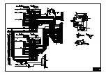
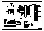
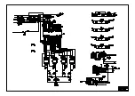
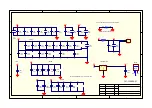
Page 32: ...L30K9A W SCH...

Page 33: ......

Page 34: ......

Page 35: ......

Page 36: ......

Page 37: ......

Page 38: ......

Page 39: ......

Page 40: ......

Page 41: ......

Page 42: ......

Page 43: ......

Page 44: ......

Page 45: ......

Page 46: ......

Page 47: ......

Page 48: ......

Page 49: ......

Page 50: ...L40K9A SCH...

Page 51: ......

Page 52: ......

Page 53: ......

Page 54: ...F CB27 0 1UF CB16 0 1UF 1 2 CB47 100UF CB55 0 1UF CB17 0 1UF CB37 0 1UF R24 0 OHM 1 2 CB23 100UF CB40 0 1UF IN 3 OUT 2 ADJ 1 N13 2830 3 3V CB36 0 1UF CB4 0 1UF CB5 0 1UF 1 2 CB22 10UF 1 2 X2 Power 1 2...

Page 55: ...R22 33OHM D0 3 D1 4 D2 7 D3 8 D4 13 D5 14 D6 17 D7 18 OC 1 CLK 11 Q0 2 Q1 5 Q2 6 Q3 9 Q4 12 Q5 15 Q6 16 Q7 19 N2 74HCT374 V1 FDN338P 1 2 C5 100UF 1 2 C7 47UF C8 0 1UF C14 0 1UF C12 0 1UF R11 10K V2 F...

Page 56: ...LA18 LA4 LA2 LA9 LD6 LD5 LD7 LD0 RST LA5 LA16 LA17 LA11 LA10 LD3 LD1 LA13 LA15 LA3 LA8 LA0 LA21 LA19 LA6 LD4 LA12 LA7 LA1 LD2 LA14 LD 0 7 LA 0 19 LD 0 7 A0 12 A1 11 A2 10 A3 9 A4 8 A5 7 A6 6 A7 5 A8 2...

Page 57: ...DMA7 62 DMA8 63 DMA9 64 DMA10 65 DMA11 66 VSS 67 DCAS 69 DSCK DOE 70 DWE 71 DRAS0 72 DBANK0 DRAS1 73 DBANK1 DRAS2 74 VSS 76 DB0 77 DB1 78 DB2 79 DB3 80 DB4 81 DB5 82 VSS 84 DB6 85 DB7 86 DB8 87 DB9 8...

Page 58: ......

Reviews: