


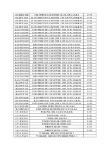
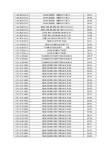
9
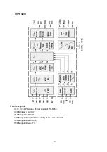
IC BLOCK DIAGRAM
1.MSP3420
Pins description:
2,3 PIN:SCL,SDA applied for control the operation of IC .
27,28 PIN:output left and right sound channel R/L to speaker processor.
36,37 PIN:AV OUT of sound R/L.
47,48 PIN:
DVI/YPbPr1/YPbPr2
selected input R/L.
50,51 PIN:Input of VGA. R/L
53,54 PIN:Input of AV2 R/L.
56,57 PIN:Input R/L of
AV1/SVHS
67 PIN:Input TV SIF.
Summary of Contents for LC27K6
Page 1: ...COLOR TELEVISION LC27K6 ...
Page 13: ...11 3 JAG ASM ...
Page 15: ...13 ...
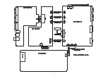
Page 18: ...EXPLODED VIEW 16 ...
Page 53: ......
Page 54: ......
Page 55: ......
Page 56: ......
Page 57: ......
Page 58: ......
Page 59: ......
Page 60: ......
Page 61: ......
Page 62: ......
Page 63: ......
Page 64: ......
Page 65: ......
Page 66: ......
Page 67: ......
Page 68: ......
Page 69: ......
Page 70: ......
Page 71: ......
Page 72: ......
Page 73: ......


