Summary of Contents for LC30B1
Page 1: ...COLOR TELEVISION LC30B1 ...
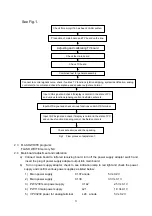
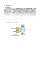
Page 12: ......
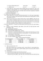
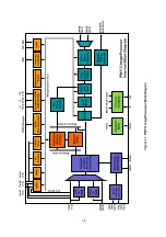
Page 14: ...12 ...
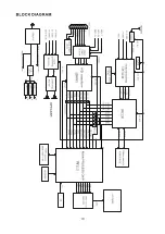
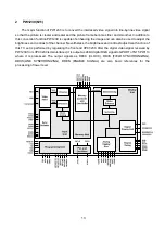
Page 19: ...17 9 K4S641632C N12 10 DS90C383A N16 D S 90C 383A D S 90C F383A ...
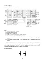
Page 20: ...18 11 Z86129 N8 ...
Page 21: ...19 12 LVC16244 N13 N14 13 PI5330 N1 14 74LV126 N4 ...
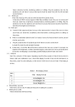
Page 22: ......
Page 28: ...26 EXPLODED VIEWS 1 2 3 4 5 6 7 8 9 10 11 12 13 14 15 16 17 18 19 ...
Page 30: ......
Page 31: ......
Page 32: ......
Page 33: ......
Page 34: ......
Page 35: ......
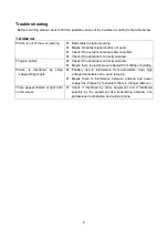
Page 36: ......


