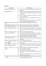
1
1
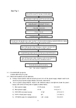
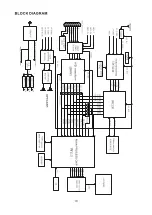
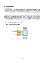
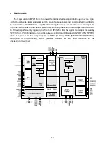
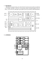
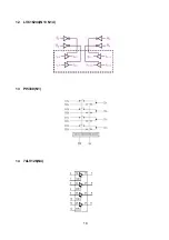
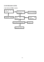
IC Block Diagram
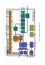
1 PW113(N15)
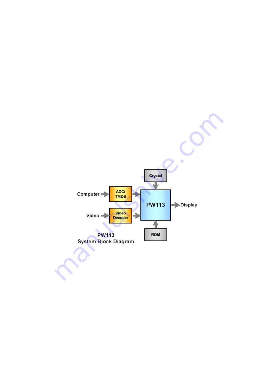
PW113 is the MCU of this TV set and is also its core chip. It communicates with various other chips
by means of bus line 12. The work it performs includes picture scaling (SCALER), receiving of external
control signals, sending of various control signals to corresponding signal processing chips so as to
complete relevant functions. Picture signal is input through GPORT of PW113 to SCALER for processing.
The processed signal is output through GPORT as R,G,B signal and D-HS (line synchronizing), D-VS
(field synchronizing), DCLK (82 MHz clock signal) and D-EN (enable signal). The external control signal
received by PW113 includes IRIN of Pin203 (signal received by remote control), KEY [2-7] of PORTA
(push key control signal) and reset signal etc. Major control signals output from PW113 include backlight
control signal BKLON(Pin 40), Panel power supply control signal LCDON(Pin 39), PI5V330 selective
control signal VAGSEL(Pin 43), backlight adjustment signal PWMOUT(Pin 200), power amplification
mute control signal MUTE(Pin 201), LED lamp control signal LED7(Pin 46, to be high electric level when
switched on) and selective signals for certain chips.
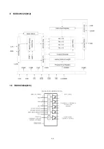
Block diagram for PW113 system
Summary of Contents for LC30B1
Page 1: ...COLOR TELEVISION LC30B1 ...
Page 12: ......
Page 14: ...12 ...
Page 19: ...17 9 K4S641632C N12 10 DS90C383A N16 D S 90C 383A D S 90C F383A ...
Page 20: ...18 11 Z86129 N8 ...
Page 21: ...19 12 LVC16244 N13 N14 13 PI5330 N1 14 74LV126 N4 ...
Page 22: ......
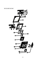
Page 28: ...26 EXPLODED VIEWS 1 2 3 4 5 6 7 8 9 10 11 12 13 14 15 16 17 18 19 ...
Page 30: ......
Page 31: ......
Page 32: ......
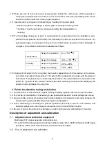
Page 33: ......
Page 34: ......
Page 35: ......
Page 36: ......


